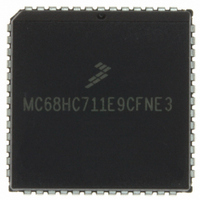
MC68HC711E9CFNE3 Freescale Semiconductor, MC68HC711E9CFNE3 Datasheet - Page 69

MC68HC711E9CFNE3
Manufacturer Part Number
MC68HC711E9CFNE3
Description
IC MCU 3MHZ 12K OPT 52-PLCC
Manufacturer
Freescale Semiconductor
Series
HC11r
Specifications of MC68HC711E9CFNE3
Core Processor
HC11
Core Size
8-Bit
Speed
3MHz
Connectivity
SCI, SPI
Peripherals
POR, WDT
Number Of I /o
38
Program Memory Size
12KB (12K x 8)
Program Memory Type
OTP
Eeprom Size
512 x 8
Ram Size
512 x 8
Voltage - Supply (vcc/vdd)
4.5 V ~ 5.5 V
Data Converters
A/D 8x8b
Oscillator Type
Internal
Operating Temperature
-40°C ~ 85°C
Package / Case
52-PLCC
Processor Series
HC711E
Core
HC11
Data Bus Width
8 bit
Data Ram Size
512 B
Interface Type
SCI, SPI
Maximum Clock Frequency
3 MHz
Number Of Programmable I/os
38
Number Of Timers
8
Maximum Operating Temperature
+ 85 C
Mounting Style
SMD/SMT
Minimum Operating Temperature
- 40 C
On-chip Adc
8 bit
Lead Free Status / RoHS Status
Lead free / RoHS Compliant
Available stocks
Company
Part Number
Manufacturer
Quantity
Price
Company:
Part Number:
MC68HC711E9CFNE3
Manufacturer:
FREESCAL
Quantity:
5 530
Company:
Part Number:
MC68HC711E9CFNE3
Manufacturer:
Freescale Semiconductor
Quantity:
10 000
- Current page: 69 of 336
- Download datasheet (4Mb)
4.4 Memory Map
M68HC11E Family — Rev. 3.2
MOTOROLA
passes to the loaded program at $0000. Refer to
Figure
Use of an external pullup resistor is required when using the SCI
transmitter pin because port D pins are configured for wired-OR
operation by the bootloader. In bootstrap mode, the interrupt vectors are
directed to RAM. This allows the use of interrupts through a jump table.
Refer to the application note AN1060 entitled
Mode, that is included in this data book.
The operating mode determines memory mapping and whether external
addresses can be accessed. Refer to
Figure
maps for each of the three families comprising the M68HC11 E series of
MCUs.
Memory locations for on-chip resources are the same for both expanded
and single-chip modes. Control bits in the configuration (CONFIG)
register allow EPROM and EEPROM (if present) to be disabled from the
memory map. The RAM is mapped to $0000 after reset. It can be placed
at any 4-Kbyte boundary ($x000) by writing an appropriate value to the
RAM and I/O map register (INIT). The 64-byte register block is mapped
to $1000 after reset and also can be placed at any 4-Kbyte boundary
($x000) by writing an appropriate value to the INIT register. If RAM and
registers are mapped to the same boundary, the first 64 bytes of RAM
will be inaccessible.
Refer to
assignments. Reset states shown are for single-chip mode only.
Operating Modes and On-Chip Memory
4-4,
4-4,
Figure
Figure
Figure
4-7, which details the MCU register and control bit
4-5, and
4-5, and
Figure
Figure
4-6.
4-6, which illustrate the memory
Figure
Operating Modes and On-Chip Memory
4-2,
M68HC11 Bootstrap
Figure
Figure
4-2,
4-3,
Technical Data
Figure
Memory Map
4-3,
69
Related parts for MC68HC711E9CFNE3
Image
Part Number
Description
Manufacturer
Datasheet
Request
R

Part Number:
Description:
APPENDIX A ELECTRICAL CHARACTERISTICS
Manufacturer:
FREESCALE [Freescale Semiconductor, Inc]
Datasheet:
Part Number:
Description:
Manufacturer:
Freescale Semiconductor, Inc
Datasheet:
Part Number:
Description:
Manufacturer:
Freescale Semiconductor, Inc
Datasheet:
Part Number:
Description:
Manufacturer:
Freescale Semiconductor, Inc
Datasheet:
Part Number:
Description:
Manufacturer:
Freescale Semiconductor, Inc
Datasheet:
Part Number:
Description:
Manufacturer:
Freescale Semiconductor, Inc
Datasheet:
Part Number:
Description:
Manufacturer:
Freescale Semiconductor, Inc
Datasheet:
Part Number:
Description:
Manufacturer:
Freescale Semiconductor, Inc
Datasheet:
Part Number:
Description:
Manufacturer:
Freescale Semiconductor, Inc
Datasheet:
Part Number:
Description:
Manufacturer:
Freescale Semiconductor, Inc
Datasheet:
Part Number:
Description:
Manufacturer:
Freescale Semiconductor, Inc
Datasheet:
Part Number:
Description:
Manufacturer:
Freescale Semiconductor, Inc
Datasheet:
Part Number:
Description:
Manufacturer:
Freescale Semiconductor, Inc
Datasheet:
Part Number:
Description:
Manufacturer:
Freescale Semiconductor, Inc
Datasheet:
Part Number:
Description:
Manufacturer:
Freescale Semiconductor, Inc
Datasheet:


