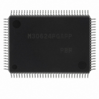
M30624FGAFP#U3 Renesas Electronics America, M30624FGAFP#U3 Datasheet - Page 238

M30624FGAFP#U3
Manufacturer Part Number
M30624FGAFP#U3
Description
IC M16C MCU FLASH 100QFP
Manufacturer
Renesas Electronics America
Series
M16C™ M16C/60r
Datasheets
1.M30622SAFPU5.pdf
(277 pages)
2.M30622SAFPU5.pdf
(617 pages)
3.M30622SAFPU5.pdf
(308 pages)
Specifications of M30624FGAFP#U3
Core Processor
M16C/60
Core Size
16-Bit
Speed
16MHz
Connectivity
SIO, UART/USART
Peripherals
DMA, PWM, WDT
Number Of I /o
85
Program Memory Size
256KB (256K x 8)
Program Memory Type
FLASH
Ram Size
20K x 8
Voltage - Supply (vcc/vdd)
4.2 V ~ 5.5 V
Data Converters
A/D 10x10b, D/A 2x8b
Oscillator Type
Internal
Operating Temperature
-40°C ~ 85°C
Package / Case
100-QFP
For Use With
867-1000 - KIT QUICK START RENESAS 62PM3062PT3-CPE-3 - EMULATOR COMPACT M16C/62P/30P
Lead Free Status / RoHS Status
Lead free / RoHS Compliant
Eeprom Size
-
Available stocks
Company
Part Number
Manufacturer
Quantity
Price
Part Number:
M30624FGAFP#U3M30624FGAFP#D3
Manufacturer:
Renesas Electronics America
Quantity:
10 000
Part Number:
M30624FGAFP#U3M30624FGAFP#D5
Manufacturer:
Renesas Electronics America
Quantity:
10 000
- Current page: 238 of 277
- Download datasheet (4Mb)
Appendix Standard Serial I/O Mode (Flash Memory Version)
Pin functions (Flash memory standard serial I/O mode)
V
X
AV
V
P5
P5
P5
P5
P6
P6
P6
P6
P10
CNV
RESET
X
BYTE
P0
P1
P2
P3
P4
P6
P7
P8
P8
P8
P9
CC
IN
REF
OUT
0
0
0
0
0
1
6,
0
5
0
4
5
6
7
0
0
CC
0
7
5
0
,V
to P0
to P1
to P2
to P3
to P4
to P5
to P6
to P7
to P9
to P8
P5
SS
, AV
to P10
SS
7
Pin
7
7
7
7
7
4,
3
7
7
SS
4
, P8
7
6
,
EPM input
BUSY output
SCLK input
TxD output
Power input
CNV
Reset input
Clock input
Clock output
BYTE
Analog power supply input
Reference voltage input
Input port P0
Input port P1
Input port P2
Input port P3
Input port P4
Input port P5
CE input
Input port P6
RxD input
Input port P7
Input port P8
NMI input
Input port P9
Input port P10
SS
Name
I/O
O
O
O
I
I
I
I
I
I
I
I
I
I
I
I
I
I
I
I
I
I
I
I
I
Apply program/erase protection voltage to Vcc pin and 0 V to Vss pin.
Connect a ceramic resonator or crystal oscillator between X
X
and open X
Connect AV
Enter the reference voltage for AD from this pin.
Input "H" or "L" level signal or open.
Input "H" or "L" level signal or open.
Input "H" or "L" level signal or open.
Input "H" or "L" level signal or open.
Input "H" or "L" level signal or open.
Input "H" or "L" level signal or open.
Input "H" or "L" level signal or open.
Standard serial I/O mode 1: BUSY signal output pin
Standard serial I/O mode 2: Monitors the boot program operation
check signal output pin.
Input "H" or "L" level signal or open.
Input "H" or "L" level signal or open.
Connect this pin to Vcc.
Input "H" or "L" level signal or open.
Input "H" or "L" level signal or open.
Connect to Vcc pin.
Reset input pin. While reset is "L" level, a 20 cycle or longer clock
must be input to X
Connect this pin to V
Input "H" level signal.
Input "L" level signal.
Standard serial I/O mode 1: Serial clock input pin
Standard serial I/O mode 2: Input "L".
Serial data input pin
Serial data output pin
OUT
pins. To input an externally generated clock, input it to X
OUT
SS
to V
pin.
IN
SS
pin.
SS
and AV
or V
SINGLE-CHIP 16-BIT CMOS MICROCOMPUTER
Description
CC
CC
.
to V
CC
, respectively.
M16C / 62A Group
Mitsubishi microcomputers
IN
and
IN
pin
235
Related parts for M30624FGAFP#U3
Image
Part Number
Description
Manufacturer
Datasheet
Request
R

Part Number:
Description:
KIT STARTER FOR M16C/29
Manufacturer:
Renesas Electronics America
Datasheet:

Part Number:
Description:
KIT STARTER FOR R8C/2D
Manufacturer:
Renesas Electronics America
Datasheet:

Part Number:
Description:
R0K33062P STARTER KIT
Manufacturer:
Renesas Electronics America
Datasheet:

Part Number:
Description:
KIT STARTER FOR R8C/23 E8A
Manufacturer:
Renesas Electronics America
Datasheet:

Part Number:
Description:
KIT STARTER FOR R8C/25
Manufacturer:
Renesas Electronics America
Datasheet:

Part Number:
Description:
KIT STARTER H8S2456 SHARPE DSPLY
Manufacturer:
Renesas Electronics America
Datasheet:

Part Number:
Description:
KIT STARTER FOR R8C38C
Manufacturer:
Renesas Electronics America
Datasheet:

Part Number:
Description:
KIT STARTER FOR R8C35C
Manufacturer:
Renesas Electronics America
Datasheet:

Part Number:
Description:
KIT STARTER FOR R8CL3AC+LCD APPS
Manufacturer:
Renesas Electronics America
Datasheet:

Part Number:
Description:
KIT STARTER FOR RX610
Manufacturer:
Renesas Electronics America
Datasheet:

Part Number:
Description:
KIT STARTER FOR R32C/118
Manufacturer:
Renesas Electronics America
Datasheet:

Part Number:
Description:
KIT DEV RSK-R8C/26-29
Manufacturer:
Renesas Electronics America
Datasheet:

Part Number:
Description:
KIT STARTER FOR SH7124
Manufacturer:
Renesas Electronics America
Datasheet:

Part Number:
Description:
KIT STARTER FOR H8SX/1622
Manufacturer:
Renesas Electronics America
Datasheet:

Part Number:
Description:
KIT DEV FOR SH7203
Manufacturer:
Renesas Electronics America
Datasheet:


