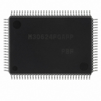
M30624FGAFP#U3 Renesas Electronics America, M30624FGAFP#U3 Datasheet - Page 30

M30624FGAFP#U3
Manufacturer Part Number
M30624FGAFP#U3
Description
IC M16C MCU FLASH 100QFP
Manufacturer
Renesas Electronics America
Series
M16C™ M16C/60r
Datasheets
1.M30622SAFPU5.pdf
(277 pages)
2.M30622SAFPU5.pdf
(617 pages)
3.M30622SAFPU5.pdf
(308 pages)
Specifications of M30624FGAFP#U3
Core Processor
M16C/60
Core Size
16-Bit
Speed
16MHz
Connectivity
SIO, UART/USART
Peripherals
DMA, PWM, WDT
Number Of I /o
85
Program Memory Size
256KB (256K x 8)
Program Memory Type
FLASH
Ram Size
20K x 8
Voltage - Supply (vcc/vdd)
4.2 V ~ 5.5 V
Data Converters
A/D 10x10b, D/A 2x8b
Oscillator Type
Internal
Operating Temperature
-40°C ~ 85°C
Package / Case
100-QFP
For Use With
867-1000 - KIT QUICK START RENESAS 62PM3062PT3-CPE-3 - EMULATOR COMPACT M16C/62P/30P
Lead Free Status / RoHS Status
Lead free / RoHS Compliant
Eeprom Size
-
Available stocks
Company
Part Number
Manufacturer
Quantity
Price
Part Number:
M30624FGAFP#U3M30624FGAFP#D3
Manufacturer:
Renesas Electronics America
Quantity:
10 000
Part Number:
M30624FGAFP#U3M30624FGAFP#D5
Manufacturer:
Renesas Electronics America
Quantity:
10 000
- Current page: 30 of 277
- Download datasheet (4Mb)
Bus Control
Bus Control
Table 1.9.1. External areas specified by the chip select signals
Note :Be sure to set bit 3 (PM13) of processor mode register 1 to “0”.
(A product having an internal RAM equal to or less than 15K bytes and a ROM equal to or less than 192K bytes)(Note)
Memory expansion mode
Microprocessor mode
The following explains the signals required for accessing external devices and software waits. The signals
required for accessing the external devices are valid when the processor mode is set to memory expansion
mode and microprocessor mode. The software waits are valid in all processor modes.
(1) Address bus/data bus
(2) Chip select signal
The address bus consists of the 20 pins A
The data bus consists of the pins for data I/O. When the BYTE pin is “H”, the 8 ports D
as the data bus. When BYTE is “L”, the 16 ports D
When a change is made from single-chip mode to memory expansion mode, the value of the address
bus is undefined until external memory is accessed.
The chip select signal is output using the same pins as P4
register (address 0008
select control register is valid in memory expansion mode and microprocessor mode. In single-chip
mode, P4
register.
In microprocessor mode, only CS0 outputs the chip select signal after the reset state has been can-
celled. CS1 to CS3 function as input ports. Figure 1.9.1 shows the chip select control register.
The chip select signal can be used to split the external area into as many as four blocks. Tables 1.9.1
and 1.9.2 show the external memory areas specified using the chip select signal.
Processor mode
_______
4
to P4
_______
7
function as programmable I/O ports regardless of the value in the chip select control
16
) set each pin to function as a port or to output the chip select signal. The chip
(640K bytes)
(832K bytes)
30000
30000
CFFFF
FFFFF
_______
CS0
16
16
16
16
to
to
0
to A
(32K bytes)
19
28000
2FFFF
for accessing the 1M bytes of address space.
0
CS1
to D
Chip select signal
16
16
15
to
4
to P4
function as the data bus.
SINGLE-CHIP 16-BIT CMOS MICROCOMPUTER
7
. Bits 0 to 3 of the chip select control
(128K bytes)
08000
27FFF
CS2
16
16
to
M16C / 62A Group
Mitsubishi microcomputers
0
(16K bytes)
04000
07FFF
to D
CS3
7
16
function
16
to
27
Related parts for M30624FGAFP#U3
Image
Part Number
Description
Manufacturer
Datasheet
Request
R

Part Number:
Description:
KIT STARTER FOR M16C/29
Manufacturer:
Renesas Electronics America
Datasheet:

Part Number:
Description:
KIT STARTER FOR R8C/2D
Manufacturer:
Renesas Electronics America
Datasheet:

Part Number:
Description:
R0K33062P STARTER KIT
Manufacturer:
Renesas Electronics America
Datasheet:

Part Number:
Description:
KIT STARTER FOR R8C/23 E8A
Manufacturer:
Renesas Electronics America
Datasheet:

Part Number:
Description:
KIT STARTER FOR R8C/25
Manufacturer:
Renesas Electronics America
Datasheet:

Part Number:
Description:
KIT STARTER H8S2456 SHARPE DSPLY
Manufacturer:
Renesas Electronics America
Datasheet:

Part Number:
Description:
KIT STARTER FOR R8C38C
Manufacturer:
Renesas Electronics America
Datasheet:

Part Number:
Description:
KIT STARTER FOR R8C35C
Manufacturer:
Renesas Electronics America
Datasheet:

Part Number:
Description:
KIT STARTER FOR R8CL3AC+LCD APPS
Manufacturer:
Renesas Electronics America
Datasheet:

Part Number:
Description:
KIT STARTER FOR RX610
Manufacturer:
Renesas Electronics America
Datasheet:

Part Number:
Description:
KIT STARTER FOR R32C/118
Manufacturer:
Renesas Electronics America
Datasheet:

Part Number:
Description:
KIT DEV RSK-R8C/26-29
Manufacturer:
Renesas Electronics America
Datasheet:

Part Number:
Description:
KIT STARTER FOR SH7124
Manufacturer:
Renesas Electronics America
Datasheet:

Part Number:
Description:
KIT STARTER FOR H8SX/1622
Manufacturer:
Renesas Electronics America
Datasheet:

Part Number:
Description:
KIT DEV FOR SH7203
Manufacturer:
Renesas Electronics America
Datasheet:


