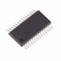
MAXQ3108-FFN+ Maxim Integrated Products, MAXQ3108-FFN+ Datasheet - Page 45

MAXQ3108-FFN+
Manufacturer Part Number
MAXQ3108-FFN+
Description
IC MCU DUAL-CORE 16BIT 28-TSSOP
Manufacturer
Maxim Integrated Products
Series
MAXQ™r
Datasheet
1.MAXQ3108-FFN.pdf
(64 pages)
Specifications of MAXQ3108-FFN+
Core Processor
RISC
Core Size
16-Bit
Speed
10MHz
Connectivity
I²C, SPI, UART/USART
Peripherals
POR, PWM, WDT
Number Of I /o
21
Program Memory Size
64KB (32K x 16)
Program Memory Type
FLASH
Ram Size
11K x 8
Voltage - Supply (vcc/vdd)
1.8 V ~ 3.6 V
Oscillator Type
External
Operating Temperature
-40°C ~ 85°C
Package / Case
28-TSSOP
Processor Series
MAXQ
Core
RISC
Data Bus Width
16 bit
Data Ram Size
2 KB
Interface Type
I2C, JTAG, SPI
Maximum Clock Frequency
10 MHz
Number Of Programmable I/os
22
Number Of Timers
2
Operating Supply Voltage
3.6 V
Maximum Operating Temperature
+ 85 C
Mounting Style
SMD/SMT
Minimum Operating Temperature
- 40 C
Lead Free Status / RoHS Status
Lead free / RoHS Compliant
Eeprom Size
-
Data Converters
-
Lead Free Status / Rohs Status
Lead free / RoHS Compliant
TB0C (05h, 04h)
Initialization:
Read/Write Access:
TB0C.[15:0]:
SCON1 (06h, 04h)
Initialization:
Read/Write Access:
SCON1.0: RI
SCON1.1: TI
SCON1.2: RB8
SCON1.3: TB8
SCON1.4: REN
SCON1.5: SM2
SCON1.6: SM1
SCON1.7: SM0/FE
SBUF1 (07h, 04h)
Initialization:
Read/Write Access:
SBUF1.[7:0]:
______________________________________________________________________________________
Low-Power, Dual-Core Microcontroller
Timer B 0 Compare
This register is cleared to 0000h on all forms of reset.
Unrestricted read/write.
Timer B Compare Bits 15:0. This register is used for comparison versus the TB0V value when
timer B is operated in compare mode.
Serial Port 1 Control Register
The serial port control is cleared to 00h on all forms of reset.
Unrestricted read/write.
Receive Interrupt Flag. This bit indicates that a data byte has been received in the serial-port
buffer. The bit is set at the end of the 8th bit for mode 0, after the last sample of the incoming stop
bit for mode 1 subject to the value of the SM2 bit, or after the last sample of RB8 for modes 2 and
3. This bit must be cleared by software once set.
Transmit Interrupt Flag. This bit indicates that the data in the serial-port data buffer has been
completely shifted out. It is set at the end of the last data bit for all modes of operation and must
be cleared by software once set.
9th Received Bit State. This bit identifies the state of the 9th bit of received data in serial-port
modes 2 and 3. When SM2 is 0, it is the state of the stop bit in mode 1. This bit has no meaning in
mode 0.
9th Transmission Bit State. This bit defines the state of the 9th transmission bit in serial-port
modes 2 and 3.
Receive Enable
Serial Port 1 Mode Bit 2. Setting this bit in mode 1 ignores reception if an invalid stop bit is
detected. Setting this bit in mode 2 or 3 enables multiprocessor communications, and prevents the
RI bit from being set and the interrupt from being asserted if the 9th bit received is 0. This bit also
used to support mode 0 for clock selection.
Serial Port 1 Mode Bit 1
Serial Port 1 Mode Bit 0/Framing Error Flag. When FEDE is 0, this bit is SM0. When FEDE is set to
1, this bit is the FE flag that is set upon detection of an invalid stop bit. It must be cleared by
software. Modification of this bit when FEDE is set has no effect on the serial mode. See the table
in the SCON0.7 bit description for guidelines.
Serial Data Buffer 1
This buffer is cleared to 00h on all forms of reset.
Unrestricted read/write.
Serial Data Buffer 1 Bit 7:0. Data for serial port 1 is read from or written to this location. The
serial transmit and receive buffers are separate but both are addressed at this location.
REN_1 = 0: Serial port 1 receiver disabled.
REN_1 = 1: Serial port 1 receiver enabled for modes 1, 2, and 3. Initiate synchronous reception
for mode 0.
SM2 = 0: clock is divided by 12.
SM2 = 1: clock is divided by 4.
Special Function Register Bit Descriptions (continued)
45


