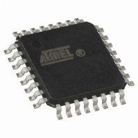
AT90LS2333-4AI Atmel, AT90LS2333-4AI Datasheet - Page 32

AT90LS2333-4AI
Manufacturer Part Number
AT90LS2333-4AI
Description
IC MCU 2K 4MHZ A/D LV IT 32TQFP
Manufacturer
Atmel
Series
AVR® 90LSr
Datasheet
1.AT90LS2333-4AC.pdf
(103 pages)
Specifications of AT90LS2333-4AI
Core Processor
AVR
Core Size
8-Bit
Speed
4MHz
Connectivity
SPI, UART/USART
Peripherals
Brown-out Detect/Reset, POR, PWM, WDT
Number Of I /o
20
Program Memory Size
2KB (1K x 16)
Program Memory Type
FLASH
Eeprom Size
128 x 8
Ram Size
128 x 8
Voltage - Supply (vcc/vdd)
2.7 V ~ 6 V
Data Converters
A/D 6x10b
Oscillator Type
Internal
Operating Temperature
-40°C ~ 85°C
Package / Case
32-TQFP, 32-VQFP
Lead Free Status / RoHS Status
Contains lead / RoHS non-compliant
•
These bits are reserved bits in the AT90S2333/4433 and always read zero.
•
These bits select PWM operation of Timer/Counter1 as specified in Table 11. This mode is described on page 34.
Table 11. PWM Mode Select
Timer/Counter1 Control Register B - TCCR1B
•
When the ICNC1 bit is cleared (zero), the input capture trigger noise canceler function is disabled. The input capture is trig-
gered at the first rising/falling edge sampled on the ICP - input capture pin - as specified. When the ICNC1 bit is set (one),
four successive samples are measured on the ICP - input capture pin, and all samples must be high/low according to the
input capture trigger specification in the ICES1 bit. The actual sampling frequency is the XTAL clock frequency.
•
While the ICES1 bit is cleared (zero), the Timer/Counter1 contents are transferred to the Input Capture Register - ICR1 - on
the falling edge of the input capture pin - ICP. While the ICES1 bit is set (one), the Timer/Counter1 contents are transferred
to the Input Capture Register - ICR1 - on the rising edge of the input capture pin - ICP.
•
These bits are reserved bits in the AT90S2333/4433 and always read zero.
•
When the CTC1 control bit is set (one), the Timer/Counter1 is reset to $0000 in the clock cycle after a compare match. If
the CTC1 control bit is cleared, Timer/Counter1 continues counting and is unaffected by a compare match. Since the com-
pare match is detected in the CPU clock cycle following the match, this function will behave differently when a prescaling
higher than 1 is used for the timer. When a prescaling of 1 is used, and the compare register is set to C, the timer will count
as follows if CTC1 is set:
... | C-2 | C-1 | C | 0 | 1 | ...
When the prescaler is set to divide by 8, the timer will count like this:
... | C-2, C-2, C-2, C-2, C-2, C-2, C-2, C-2 | C-1, C-1, C-1, C-1, C-1, C-1, C-1, C-1 | C, 0, 0, 0, 0, 0, 0, 0, 0 | ...
In PWM mode, this bit has no effect.
•
The Clock Select1 bits 2,1 and 0 define the prescaling source of Timer/Counter1.
32
Bit
$2E ($4E)
Read/Write
Initial value
Bits 5..2 - Res: Reserved bits
Bits 1,0 - PWM11, PWM10: Pulse Width Modulator Select Bits
Bit 7 - ICNC1: Input Capture1 Noise Canceler (4 CKs)
Bit 6 - ICES1: Input Capture1 Edge Select
Bits 5, 4 - Res: Reserved bits
Bit 3 - CTC1: Clear Timer/Counter1 on Compare match
Bits 2,1,0 - CS12, CS11, CS10: Clock Select1, bit 2,1 and 0
PWM11
0
0
1
1
AT90S/LS2333 and AT90S/LS4433
ICNC1
R/W
7
0
PWM10
0
1
0
1
ICES1
R/W
6
0
Description
PWM operation of Timer/Counter1 is disabled
Timer/Counter1 is an 8-bit PWM
Timer/Counter1 is a 9-bit PWM
Timer/Counter1 is a 10-bit PWM
R
5
0
-
R
4
0
-
CTC1
R/W
3
0
CS12
R/W
2
0
CS11
R/W
1
0
CS10
R/W
0
0
TCCR1B


