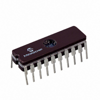
PIC16C782/JW Microchip Technology, PIC16C782/JW Datasheet - Page 13

PIC16C782/JW
Manufacturer Part Number
PIC16C782/JW
Description
IC MCU EPROM 2KX14 COMP 20CDIP
Manufacturer
Microchip Technology
Series
PIC® 16Cr
Datasheets
1.PIC16C781-ISO.pdf
(186 pages)
2.PIC16C781-ISO.pdf
(8 pages)
3.PIC16C781-ISO.pdf
(8 pages)
Specifications of PIC16C782/JW
Core Processor
PIC
Core Size
8-Bit
Speed
20MHz
Peripherals
Brown-out Detect/Reset, POR, PWM, WDT
Number Of I /o
13
Program Memory Size
3.5KB (2K x 14)
Program Memory Type
EPROM, UV
Ram Size
128 x 8
Voltage - Supply (vcc/vdd)
4 V ~ 5.5 V
Data Converters
A/D 8x8b; D/A 1x8b
Oscillator Type
Internal
Operating Temperature
0°C ~ 70°C
Package / Case
20-CDIP (0.300", 7.62mm) Window
For Use With
DVA16XP202 - ADAPTER DEVICE PIC16C781/782DM163012 - BOARD DEMO PICDEM FOR 16C781/782AC164028 - MODULE SKT PROMATEII 20SOIC/DIP
Lead Free Status / RoHS Status
Contains lead / RoHS non-compliant
Eeprom Size
-
Connectivity
-
Other names
Q1137459
Available stocks
Company
Part Number
Manufacturer
Quantity
Price
- Current page: 13 of 186
- Download datasheet (4Mb)
2.0
There are two memory blocks in each of these
PICmicro
data memory) has its own bus, so that concurrent
access can occur.
Additional information on device memory may be found
in the PICmicro™ Mid-Range Reference Manual,
(DS33023).
2.1
The PIC16C781/782 devices have a 13-bit program
counter capable of addressing an 8K x 14 program
memory space. The PIC16C781 has 1K x 14 words of
program memory. The PIC16C782 has 2K x 14 words
of program memory. Accessing a location above the
physically implemented address causes a wraparound.
The RESET vector is at 0000h and the interrupt vector
is at 0004h.
FIGURE 2-1:
Program
On-Chip
Memory
2001 Microchip Technology Inc.
CALL, RETURN
RETFIE, RETLW
MEMORY ORGANIZATION
Program Memory Organization
®
microcontrollers. Each block (program and
Interrupt Vector
RESET Vector
Stack Level 2
Stack Level 8
Stack Level 1
PC<12:0>
PIC16C781 PROGRAM
MEMORY MAP AND
STACK
Page 0
13
1FFFh
0000h
0004h
0005h
03FFh
0400h
Preliminary
FIGURE 2-2:
2.2
The data memory is partitioned into multiple banks,
which contain the General Purpose Registers and the
Special Function Registers. Bits RP0 and RP1 are
bank select bits.
= 00
= 01
= 10
= 11
Each bank extends up to 7Fh (128 bytes). The lower
locations of each bank are reserved for the Special
Function Registers. Above the Special Function Regis-
ters are the General Purpose Registers, implemented
as static RAM. All implemented banks contain Special
Function Registers. Some frequently used Special
Function Registers from one bank are mirrored in
another bank for code reduction and quicker access.
RP1 RP0
On-Chip
Program
Memory
CALL, RETURN
RETFIE, RETLW
Data Memory Organization
Bank0
Bank1
Bank2
Bank3
PIC16C781/782
(STATUS<6:5>)
Interrupt Vector
RESET Vector
Stack Level 2
Stack Level 8
Stack Level 1
PIC16C782 PROGRAM
MEMORY MAP AND
STACK
PC<12:0>
Page 0
13
DS41171A-page 11
1FFFh
0000h
0004h
0005h
07FFh
0800h
Related parts for PIC16C782/JW
Image
Part Number
Description
Manufacturer
Datasheet
Request
R

Part Number:
Description:
3.5KB Flash, 128B RAM, 18 I/O, CLC, CWG, DDS, 10-bit ADC 20 QFN 4x4mm TUBE
Manufacturer:
Microchip Technology
Datasheet:

Part Number:
Description:
3.5KB Flash, 128B RAM, 18 I/O, CLC, CWG, DDS, 10-bit ADC 20 PDIP .300in TUBE
Manufacturer:
Microchip Technology
Datasheet:

Part Number:
Description:
3.5KB Flash, 128B RAM, 18 I/O, CLC, CWG, DDS, 10-bit ADC 20 SOIC .300in TUBE
Manufacturer:
Microchip Technology
Datasheet:

Part Number:
Description:
3.5KB Flash, 128B RAM, 18 I/O, CLC, CWG, DDS, 10-bit ADC 20 SSOP .209in TUBE
Manufacturer:
Microchip Technology
Datasheet:

Part Number:
Description:
3.5KB Flash, 128B RAM, 18 I/O, CLC, CWG, DDS, 10-bit ADC 20 QFN 4x4mm TUBE
Manufacturer:
Microchip Technology
Datasheet:

Part Number:
Description:
3.5KB Flash, 128B RAM, 18 I/O, CLC, CWG, DDS, 10-bit ADC 20 PDIP .300in TUBE
Manufacturer:
Microchip Technology
Datasheet:

Part Number:
Description:
3.5KB Flash, 128B RAM, 18 I/O, CLC, CWG, DDS, 10-bit ADC 20 SOIC .300in TUBE
Manufacturer:
Microchip Technology
Datasheet:

Part Number:
Description:
3.5KB Flash, 128B RAM, 18 I/O, CLC, CWG, DDS, 10-bit ADC 20 SSOP .209in TUBE
Manufacturer:
Microchip Technology
Datasheet:

Part Number:
Description:
3.5KB Flash, 128B RAM, 18 I/O, CLC, CWG, DDS, 10-bit ADC 20 QFN 4x4mm T/R
Manufacturer:
Microchip Technology
Datasheet:

Part Number:
Description:
3.5KB Flash, 128B RAM, 18 I/O, CLC, CWG, DDS, 10-bit ADC 20 SOIC .300in T/R
Manufacturer:
Microchip Technology
Datasheet:

Part Number:
Description:
3.5KB Flash, 128B RAM, 18 I/O, CLC, CWG, DDS, 10-bit ADC 20 SSOP .209in T/R
Manufacturer:
Microchip Technology
Datasheet:

Part Number:
Description:
3.5KB Flash, 128B RAM, 18 I/O, CLC, CWG, DDS, 10-bit ADC 20 QFN 4x4mm TUBE
Manufacturer:
Microchip Technology
Datasheet:

Part Number:
Description:
3.5KB Flash, 128B RAM, 18 I/O, CLC, CWG, DDS, 10-bit ADC 20 PDIP .300in TUBE
Manufacturer:
Microchip Technology
Datasheet:

Part Number:
Description:
3.5KB Flash, 128B RAM, 18 I/O, CLC, CWG, DDS, 10-bit ADC 20 SOIC .300in TUBE
Manufacturer:
Microchip Technology
Datasheet:

Part Number:
Description:
3.5KB Flash, 128B RAM, 18 I/O, CLC, CWG, DDS, 10-bit ADC 20 SSOP .209in TUBE
Manufacturer:
Microchip Technology
Datasheet:


