PIC16C782/JW Microchip Technology, PIC16C782/JW Datasheet - Page 77
PIC16C782/JW
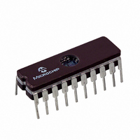
Manufacturer Part Number
PIC16C782/JW
Description
IC MCU EPROM 2KX14 COMP 20CDIP
Manufacturer
Microchip Technology
Series
PIC® 16Cr
Datasheets
1.PIC16C781-ISO.pdf
(186 pages)
2.PIC16C781-ISO.pdf
(8 pages)
3.PIC16C781-ISO.pdf
(8 pages)
Specifications of PIC16C782/JW
Core Processor
PIC
Core Size
8-Bit
Speed
20MHz
Peripherals
Brown-out Detect/Reset, POR, PWM, WDT
Number Of I /o
13
Program Memory Size
3.5KB (2K x 14)
Program Memory Type
EPROM, UV
Ram Size
128 x 8
Voltage - Supply (vcc/vdd)
4 V ~ 5.5 V
Data Converters
A/D 8x8b; D/A 1x8b
Oscillator Type
Internal
Operating Temperature
0°C ~ 70°C
Package / Case
20-CDIP (0.300", 7.62mm) Window
For Use With
DVA16XP202 - ADAPTER DEVICE PIC16C781/782DM163012 - BOARD DEMO PICDEM FOR 16C781/782AC164028 - MODULE SKT PROMATEII 20SOIC/DIP
Lead Free Status / RoHS Status
Contains lead / RoHS non-compliant
Eeprom Size
-
Connectivity
-
Other names
Q1137459
Available stocks
Company
Part Number
Manufacturer
Quantity
Price


9.4.1
Not all applications require a result having 8-bits of res-
olution. Some may instead, require a faster conversion
time. The ADC module allows users to make a trade-off
of conversion speed for resolution. Regardless of the
resolution required, the acquisition time is the same. To
speed up the conversion, the clock source of the ADC
module may be switched during the conversion, so that
the T
the applicable Electrical Specification). Once the switch
is made, all the following ADC result bits are invalid
(see ADC Conversion Timing in the Electrical Specifi-
cations section). The clock source may only be
switched between the three oscillator options (it cannot
be switched from/to RC). The equation to determine
the time before the oscillator must be switched for a
desired resolution is as follows:
Conversion time = 2T
Where: N = number of bits of resolution required.
Since the T
must employ some method (such as a timer, software
loop, etc.) to determine when the ADC oscillator must
be changed.
9.5
The ADC module can operate during SLEEP mode.
This requires that the ADC clock source be set to RC
(ADCS1:ADCS0 = 11). When the RC clock source is
selected, the ADC module waits one instruction cycle
before starting the conversion. This allows the SLEEP
instruction to be executed, which eliminates all digital
switching noise from the conversion. When the conver-
sion is completed the GO/DONE bit is cleared, and the
result is loaded into the ADRES register. If the ADC
interrupt is enabled, the device awakens from SLEEP.
If the ADC interrupt is not enabled, the ADC module is
turned off, although the ADON bit remains set.
When the ADC clock source is another clock option
(not RC), a SLEEP instruction causes the present con-
version to be aborted and the ADC module to be turned
off. The ADON bit remains set.
Turning off the ADC places the ADC module in its low-
est current consumption state.
Note:
2001 Microchip Technology Inc.
AD
time violates the minimum specified time (see
ADC Operation During SLEEP
AD
For the ADC module to operate in SLEEP,
the A/D clock source must be set to RC
(ADCS1:ADCS0 = 11). To perform an ADC
conversion in SLEEP, ensure the SLEEP
instruction immediately follows the instruc-
tion that sets the GO/DONE bit.
FASTER CONVERSION/LOWER
RESOLUTION TRADE-OFF
is based on the device oscillator, the user
AD
+ N • T
AD
+ (8 - N)(2T
OSC
)
Preliminary
9.6
The absolute accuracy (absolute error) specified for the
ADC converter includes the sum of all contributions for:
• Offset error
• Gain error
• Quantization error
• Integral non-linearity error
• Differential non-linearity error
• Monotonicity
The absolute error is defined as the maximum devia-
tion from an actual transition versus an ideal transition
for any code. The absolute error of the ADC converter
is specified as < ±1 LSb for ADC
device’s specified operating range). However, the
accuracy of the ADC converter degrades as V
diverges from V
For a given range of analog inputs, the output digital
code will be the same. This is due to the quantization of
the analog input to a digital code. Quantization error
is typically ± 1/2 LSb and is inherent in the analog to
digital conversion process. The only way to reduce
quantization error is to use an ADC with greater resolu-
tion of the ADC converter.
Offset error measures the first actual transition of a
code versus the first ideal transition of a code. Offset
error shifts the entire transfer function. Offset error can
be calibrated out of a system, or introduced into a sys-
tem, through the interaction of the total leakage current
and source impedance at the analog input.
Gain error measures the maximum deviation of the
last actual transition and the last ideal transition
adjusted for offset error. This error appears as a
change in slope of the transfer function. The difference
in gain error to full scale error is that full scale does not
take offset error into account. Gain error can be cali-
brated out in software.
Linearity error refers to the uniformity of the code
changes. Linearity errors cannot be calibrated out of
the system. Integral non-linearity error measures the
actual code transition versus the ideal code transition,
adjusted by the gain error for each code. Differential
non-linearity measures the maximum actual code
width versus the ideal code width. This measure is
unadjusted.
If the linearity errors are very large, the ADC may
become non-monotonic. This occurs when the digital
values for one or more input voltages are less than the
value for a lower input voltage.
ADC Accuracy/Error
PIC16C781/782
REF
.
REF
DS41171A-page 75
= V
DD
(over the
DD
Related parts for PIC16C782/JW
Image
Part Number
Description
Manufacturer
Datasheet
Request
R

Part Number:
Description:
3.5KB Flash, 128B RAM, 18 I/O, CLC, CWG, DDS, 10-bit ADC 20 QFN 4x4mm TUBE
Manufacturer:
Microchip Technology
Datasheet:

Part Number:
Description:
3.5KB Flash, 128B RAM, 18 I/O, CLC, CWG, DDS, 10-bit ADC 20 PDIP .300in TUBE
Manufacturer:
Microchip Technology
Datasheet:

Part Number:
Description:
3.5KB Flash, 128B RAM, 18 I/O, CLC, CWG, DDS, 10-bit ADC 20 SOIC .300in TUBE
Manufacturer:
Microchip Technology
Datasheet:

Part Number:
Description:
3.5KB Flash, 128B RAM, 18 I/O, CLC, CWG, DDS, 10-bit ADC 20 SSOP .209in TUBE
Manufacturer:
Microchip Technology
Datasheet:
Part Number:
Description:
3.5KB Flash, 128B RAM, 18 I/O, CLC, CWG, DDS, 10-bit ADC 20 QFN 4x4mm TUBE
Manufacturer:
Microchip Technology
Datasheet:
Part Number:
Description:
3.5KB Flash, 128B RAM, 18 I/O, CLC, CWG, DDS, 10-bit ADC 20 PDIP .300in TUBE
Manufacturer:
Microchip Technology
Datasheet:
Part Number:
Description:
3.5KB Flash, 128B RAM, 18 I/O, CLC, CWG, DDS, 10-bit ADC 20 SOIC .300in TUBE
Manufacturer:
Microchip Technology
Datasheet:
Part Number:
Description:
3.5KB Flash, 128B RAM, 18 I/O, CLC, CWG, DDS, 10-bit ADC 20 SSOP .209in TUBE
Manufacturer:
Microchip Technology
Datasheet:
Part Number:
Description:
3.5KB Flash, 128B RAM, 18 I/O, CLC, CWG, DDS, 10-bit ADC 20 QFN 4x4mm T/R
Manufacturer:
Microchip Technology
Datasheet:
Part Number:
Description:
3.5KB Flash, 128B RAM, 18 I/O, CLC, CWG, DDS, 10-bit ADC 20 SOIC .300in T/R
Manufacturer:
Microchip Technology
Datasheet:
Part Number:
Description:
3.5KB Flash, 128B RAM, 18 I/O, CLC, CWG, DDS, 10-bit ADC 20 SSOP .209in T/R
Manufacturer:
Microchip Technology
Datasheet:
Part Number:
Description:
3.5KB Flash, 128B RAM, 18 I/O, CLC, CWG, DDS, 10-bit ADC 20 QFN 4x4mm TUBE
Manufacturer:
Microchip Technology
Datasheet:
Part Number:
Description:
3.5KB Flash, 128B RAM, 18 I/O, CLC, CWG, DDS, 10-bit ADC 20 PDIP .300in TUBE
Manufacturer:
Microchip Technology
Datasheet:
Part Number:
Description:
3.5KB Flash, 128B RAM, 18 I/O, CLC, CWG, DDS, 10-bit ADC 20 SOIC .300in TUBE
Manufacturer:
Microchip Technology
Datasheet:
Part Number:
Description:
3.5KB Flash, 128B RAM, 18 I/O, CLC, CWG, DDS, 10-bit ADC 20 SSOP .209in TUBE
Manufacturer:
Microchip Technology
Datasheet: