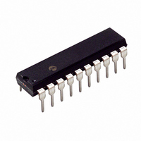
PIC16C432-E/P Microchip Technology, PIC16C432-E/P Datasheet - Page 22

PIC16C432-E/P
Manufacturer Part Number
PIC16C432-E/P
Description
IC MCU CMOS 8-BIT 20MHZ 2K 20DIP
Manufacturer
Microchip Technology
Series
PIC® 16Cr
Specifications of PIC16C432-E/P
Core Processor
PIC
Core Size
8-Bit
Speed
20MHz
Connectivity
LIN (Local Interconnect Network)
Peripherals
Brown-out Detect/Reset, POR, WDT
Number Of I /o
12
Program Memory Size
3.5KB (2K x 14)
Program Memory Type
OTP
Ram Size
128 x 8
Voltage - Supply (vcc/vdd)
4.5 V ~ 5.5 V
Oscillator Type
External
Operating Temperature
-40°C ~ 125°C
Package / Case
20-DIP (0.300", 7.62mm)
For Use With
AC164029 - MODULE SKT PROMATEII 20DIP/SSOPDVA16XP201 - ADAPTER DEVICE FOR MPLAB-ICE
Lead Free Status / RoHS Status
Request inventory verification / Request inventory verification
Eeprom Size
-
Data Converters
-
PIC16C432
4.2
PORTB is an 8-bit wide, bi-directional port. The
corresponding data direction register is TRISB. A ’1’ in
the TRISB register puts the corresponding output driver
in a High Impedance mode. A ’0’ in the TRISB register
puts the contents of the output latch on the selected
pin(s).
Reading PORTB register reads the status of the pins,
whereas writing to it will write to the port latch. All write
operations are read-modify-write operations. So a write
to a port implies that the port pins are first read, then
this value is modified and written to the port data latch.
Each of the PORTB pins has a weak internal pull-up
( 200 A typical). A single control bit can turn on all the
pull-ups. This is done by clearing the RBPU
(OPTION<7>) bit. The weak pull-up is automatically
turned off when the port pin is configured as an output.
The pull-ups are disabled on Power-on Reset.
Four of PORTB’s pins, RB<7:4>, have an interrupt-on-
change feature. Only pins configured as inputs can
cause this interrupt to occur (i.e., any RB<7:4> pin con-
figured as an output is excluded from the interrupt-on-
change comparison). The input pins of RB<7:4> are
compared with the old value latched on the last read of
PORTB. The “mismatch” outputs of RB<7:4> are
OR’ed together to generate the RBIF interrupt (flag
latched in INTCON<0>).
FIGURE 4-5:
DS41140B-page 20
Set RBIF
Data Bus
WR PORTB
WR TRISB
RBPU
RB<7:6> in Serial Programming mode
Note
(1)
From other
RB<7:4> pins
1:
PORTB and TRISB Registers
(1)
TRISB = 1 enables weak pull-up if RBPU = 0
(OPTION<7>).
RD TRISB
RD PORTB
Data Latch
TRIS Latch
D
D
CK
CK
BLOCK DIAGRAM OF
RB<7:4> PINS
Q
Q
Q
Q
Latch
EN
EN
D
D
TTL
Input
Buffer
Pull-up
Weak
V
RD Port
P
DD
ST
Buffer
I/O pin
Preliminary
This interrupt can wake the device from SLEEP. The
user, in the Interrupt Service Routine, can clear the
interrupt in the following manner:
a)
b)
A mismatch condition will continue to set flag bit RBIF.
Reading PORTB will end the mismatch condition and
allow flag bit RBIF to be cleared.
This interrupt-on-mismatch feature, together with
software configurable pull-ups on these four pins, allow
easy interface to a key pad and make it possible for
wake-up on key depression. (See AN552, “Implement-
ing Wake-up on Key Strokes”.)
The interrupt-on-change feature is recommended for
wake-up on key depression operation and operations
where PORTB is only used for the interrupt-on-change
feature. Polling of PORTB is not recommended while
using the interrupt-on-change feature.
FIGURE 4-6:
Data Bus
WR TRISB
WR PORTB
RBPU
Note:
RB0/INT
Note
Any read or write of PORTB. This will end the
mismatch condition.
Clear flag bit RBIF.
(1)
1:
(1)
If a change on the I/O pin should occur
when the read operation is being executed
(start of the Q2 cycle), then the RBIF inter-
rupt flag may not get set.
TRISB = 1 enables weak pull-up if RBPU = 0
(OPTION<7>).
RD TRISB
RD PORTB
TRIS Latch
Data Latch
D
D
CK
CK
ST
Buffer
BLOCK DIAGRAM OF
RB<3:0> PINS
Q
Q
2002 Microchip Technology Inc.
Q
EN
Pull-up
Weak
TTL
Input
Buffer
D
V
P
DD
RD Port
I/O pin


