PIC16C432-E/P Microchip Technology, PIC16C432-E/P Datasheet - Page 60
PIC16C432-E/P
Manufacturer Part Number
PIC16C432-E/P
Description
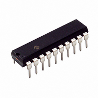
IC MCU CMOS 8-BIT 20MHZ 2K 20DIP
Manufacturer
Microchip Technology
Series
PIC® 16Cr
Specifications of PIC16C432-E/P
Core Processor
PIC
Core Size
8-Bit
Speed
20MHz
Connectivity
LIN (Local Interconnect Network)
Peripherals
Brown-out Detect/Reset, POR, WDT
Number Of I /o
12
Program Memory Size
3.5KB (2K x 14)
Program Memory Type
OTP
Ram Size
128 x 8
Voltage - Supply (vcc/vdd)
4.5 V ~ 5.5 V
Oscillator Type
External
Operating Temperature
-40°C ~ 125°C
Package / Case
20-DIP (0.300", 7.62mm)
For Use With
AC164029 - MODULE SKT PROMATEII 20DIP/SSOPDVA16XP201 - ADAPTER DEVICE FOR MPLAB-ICE
Lead Free Status / RoHS Status
Request inventory verification / Request inventory verification
Eeprom Size
-
Data Converters
-


PIC16C432
FIGURE 9-18:
9.9
If
programmed, the on-chip program memory can be
read out for verification purposes.
9.10
Four memory locations (2000h-2003h) are designated
as ID locations where the user can store checksum or
other code identification numbers. These locations are
not accessible during normal execution, but are
readable and writable during program/verify. Only the
Least Significant 4 bits of the ID locations are used.
9.11
The PIC16C432 microcontroller can be serially
programmed while in the end application circuit. This is
simply done with two lines for clock and data, and three
other lines for power, ground, and the programming
voltage. This allows customers to manufacture boards
with unprogrammed devices, and then program the
microcontroller just before shipping the product. This
also allows the most recent firmware or a custom
firmware to be programmed.
The device is placed into a Program/Verify mode by
holding the RB6 and RB7 pins low, while raising the
MCLR (V
specification). RB6 becomes the programming clock
and RB7 becomes the programming data. Both RB6
and RB7 are Schmitt Trigger inputs in this mode.
DS41140B-page 58
Note 1: XT, HS or LP Oscillator mode assumed.
INSTRUCTION FLOW
Note:
INTF flag
(INTCON<1>)
GIE bit
(INTCON<7>)
the
Instruction
Fetched
CLKOUT(4)
Instruction
Executed
2: T
3: GIE = ’1’ assumed. In this case after wake-up, the processor jumps to the interrupt routine. If GIE = ’0’, execution will continue in-line.
4: CLKOUT is not available in these osc modes, but shown here for timing reference.
INT pin
OSC1
OST
Code Protection
ID Locations
In-Circuit Serial Programming
PC
code
PP
= 1024T
Microchip does not recommend code
protecting windowed devices.
) pin from V
Inst(PC) = SLEEP
Q1 Q2 Q3 Q4
Inst(PC - 1)
OSC
protection
PC
(drawing not to scale). This delay does not occur for RC Osc mode.
WAKE-UP FROM SLEEP THROUGH INTERRUPT
IL
to V
Q1 Q2 Q3 Q4
bit(s)
Inst(PC + 1)
SLEEP
PC+1
IHH
(see programming
have
Q1
Processor in
SLEEP
not
PC+2
been
Preliminary
T
OST
(2)
Q1 Q2 Q3 Q4 Q1 Q2 Q3 Q4
Inst(PC + 2)
Inst(PC + 1)
After RESET, to place the device into Programming/
Verify mode, the program counter (PC) is at location
00h. A 6-bit command is then supplied to the device.
Depending on the command, 14-bits of program data
are then supplied to or from the device, depending if
the command was a load or a read. For complete
details of serial programming, please refer to the
PIC16C6X/7X/9XX Programming Specifications (Liter-
ature #DS30228).
A typical in-circuit serial programming connection is
shown in Figure 9-19.
FIGURE 9-19:
PC+2
External
Connector
Signals
Data I/O
CLK
+5V
V
0V
PP
Interrupt Latency
Dummy cycle
PC + 2
To Normal
Connections
To Normal
Connections
TYPICAL IN-CIRCUIT
SERIAL PROGRAMMING
CONNECTION
Q1 Q2 Q3 Q4
Inst(0004h)
Dummy cycle
2002 Microchip Technology Inc.
0004h
V
V
MCLR/V
RB6
RB7
V
Q1 Q2 Q3 Q4
DD
SS
DD
PIC16C432
Inst(0005h)
Inst(0004h)
0005h
PP
Related parts for PIC16C432-E/P
Image
Part Number
Description
Manufacturer
Datasheet
Request
R

Part Number:
Description:
3.5KB Flash, 128B RAM, 18 I/O, CLC, CWG, DDS, 10-bit ADC 20 QFN 4x4mm TUBE
Manufacturer:
Microchip Technology
Datasheet:

Part Number:
Description:
3.5KB Flash, 128B RAM, 18 I/O, CLC, CWG, DDS, 10-bit ADC 20 PDIP .300in TUBE
Manufacturer:
Microchip Technology
Datasheet:

Part Number:
Description:
3.5KB Flash, 128B RAM, 18 I/O, CLC, CWG, DDS, 10-bit ADC 20 SOIC .300in TUBE
Manufacturer:
Microchip Technology
Datasheet:

Part Number:
Description:
3.5KB Flash, 128B RAM, 18 I/O, CLC, CWG, DDS, 10-bit ADC 20 SSOP .209in TUBE
Manufacturer:
Microchip Technology
Datasheet:
Part Number:
Description:
3.5KB Flash, 128B RAM, 18 I/O, CLC, CWG, DDS, 10-bit ADC 20 QFN 4x4mm TUBE
Manufacturer:
Microchip Technology
Datasheet:
Part Number:
Description:
3.5KB Flash, 128B RAM, 18 I/O, CLC, CWG, DDS, 10-bit ADC 20 PDIP .300in TUBE
Manufacturer:
Microchip Technology
Datasheet:
Part Number:
Description:
3.5KB Flash, 128B RAM, 18 I/O, CLC, CWG, DDS, 10-bit ADC 20 SOIC .300in TUBE
Manufacturer:
Microchip Technology
Datasheet:
Part Number:
Description:
3.5KB Flash, 128B RAM, 18 I/O, CLC, CWG, DDS, 10-bit ADC 20 SSOP .209in TUBE
Manufacturer:
Microchip Technology
Datasheet:
Part Number:
Description:
3.5KB Flash, 128B RAM, 18 I/O, CLC, CWG, DDS, 10-bit ADC 20 QFN 4x4mm T/R
Manufacturer:
Microchip Technology
Datasheet:
Part Number:
Description:
3.5KB Flash, 128B RAM, 18 I/O, CLC, CWG, DDS, 10-bit ADC 20 SOIC .300in T/R
Manufacturer:
Microchip Technology
Datasheet:
Part Number:
Description:
3.5KB Flash, 128B RAM, 18 I/O, CLC, CWG, DDS, 10-bit ADC 20 SSOP .209in T/R
Manufacturer:
Microchip Technology
Datasheet:
Part Number:
Description:
3.5KB Flash, 128B RAM, 18 I/O, CLC, CWG, DDS, 10-bit ADC 20 QFN 4x4mm TUBE
Manufacturer:
Microchip Technology
Datasheet:
Part Number:
Description:
3.5KB Flash, 128B RAM, 18 I/O, CLC, CWG, DDS, 10-bit ADC 20 PDIP .300in TUBE
Manufacturer:
Microchip Technology
Datasheet:
Part Number:
Description:
3.5KB Flash, 128B RAM, 18 I/O, CLC, CWG, DDS, 10-bit ADC 20 SOIC .300in TUBE
Manufacturer:
Microchip Technology
Datasheet:
Part Number:
Description:
3.5KB Flash, 128B RAM, 18 I/O, CLC, CWG, DDS, 10-bit ADC 20 SSOP .209in TUBE
Manufacturer:
Microchip Technology
Datasheet: