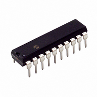
PIC16C432-E/P Microchip Technology, PIC16C432-E/P Datasheet - Page 29

PIC16C432-E/P
Manufacturer Part Number
PIC16C432-E/P
Description
IC MCU CMOS 8-BIT 20MHZ 2K 20DIP
Manufacturer
Microchip Technology
Series
PIC® 16Cr
Specifications of PIC16C432-E/P
Core Processor
PIC
Core Size
8-Bit
Speed
20MHz
Connectivity
LIN (Local Interconnect Network)
Peripherals
Brown-out Detect/Reset, POR, WDT
Number Of I /o
12
Program Memory Size
3.5KB (2K x 14)
Program Memory Type
OTP
Ram Size
128 x 8
Voltage - Supply (vcc/vdd)
4.5 V ~ 5.5 V
Oscillator Type
External
Operating Temperature
-40°C ~ 125°C
Package / Case
20-DIP (0.300", 7.62mm)
For Use With
AC164029 - MODULE SKT PROMATEII 20DIP/SSOPDVA16XP201 - ADAPTER DEVICE FOR MPLAB-ICE
Lead Free Status / RoHS Status
Request inventory verification / Request inventory verification
Eeprom Size
-
Data Converters
-
6.0
The Timer0 module timer/counter has the following
features:
• 8-bit timer/counter
• Readable and writable
• 8-bit software programmable prescaler
• Internal or external clock select
• Interrupt on overflow from FFh to 00h
• Edge select for external clock
Figure 6-1 is a simplified block diagram of the Timer0
module.
Timer mode is selected by clearing the T0CS bit
(OPTION<5>). In Timer mode, the TMR0 will increment
every instruction cycle (without prescaler). If Timer0 is
written, the increment is inhibited for the following two
cycles (Figure 6-2 and Figure 6-3). The user can work
around this by writing an adjusted value to TMR0.
Counter mode is selected by setting the T0CS bit. In
this mode, Timer0 will increment either on every rising
or falling edge of pin RA4/T0CKI. The incrementing
edge is determined by the source edge (T0SE) control
FIGURE 6-1:
FIGURE 6-2:
2002 Microchip Technology Inc.
RA4/T0CKI
PC
(Program
Counter)
Instruction
TMR0
Fetch
Instruction
Executed
Note 1: Bits T0SE, T0CS, PS2, PS1, PS0 and PSA are located in the OPTION register.
pin
TIMER0 MODULE
2: The prescaler is shared with the Watchdog Timer (Figure 6-6).
T0SE
Q1 Q2 Q3 Q4 Q1 Q2 Q3 Q4 Q1 Q2 Q3 Q4 Q1 Q2 Q3 Q4 Q1 Q2 Q3 Q4 Q1 Q2 Q3 Q4 Q1 Q2 Q3 Q4 Q1 Q2 Q3 Q4
T0
F
OSC
PC-1
TIMER0 BLOCK DIAGRAM
/4
TIMER0 (TMR0) TIMING: INTERNAL CLOCK/NO PRESCALER
MOVWF TMR0
T0+1
T0CS
PC
0
1
Write TMR0
executed
MOVF TMR0,W
T0+2
Programmable
PS<2:0>
PC+1
Prescaler
Preliminary
MOVF TMR0,W
Read TMR0
reads NT0
PC+2
PSA
1
0
NT0
bit (OPTION<4>). Clearing the T0SE bit selects the
rising edge. Restrictions on the external clock input are
discussed in detail in Section 6.2.
The prescaler is shared between the Timer0 module
and the Watchdog Timer. The prescaler assignment is
controlled in software by the control bit PSA
(OPTION<3>). Clearing the PSA bit will assign the
prescaler to Timer0. The prescaler is not readable or
writable. When the prescaler is assigned to the Timer0
module, prescale values of 1:2, 1:4,..., 1:256 are
selectable. Section 6.3 details the operation of the
prescaler.
6.1
Timer0 interrupt is generated when the TMR0 register
timer/counter overflows from FFh to 00h. This overflow
sets the T0IF bit. The interrupt can be masked by
clearing the T0IE bit (INTCON<5>). The T0IF bit
(INTCON<2>) must be cleared in software by the
Timer0 module Interrupt Service Routine, before re-
enabling this interrupt. The Timer0 interrupt cannot
wake the processor from SLEEP, since the timer is
shut-off during SLEEP. See Figure 6-4 for Timer0 inter-
rupt timing.
PS
MOVF TMR0,W
Read TMR0
reads NT0
OUT
PC+3
(2 T
Sync with
Timer0 Interrupt
Internal
clocks
CY
MOVF TMR0,W
delay)
Read TMR0
reads NT0
PC+4
PS
OUT
MOVF TMR0,W
Read TMR0
reads NT0 + 1
PIC16C432
NT0+1
Data Bus
TMR0
PC+5
8
DS41140B-page 27
Set Flag bit T0IF
NT0+2
Read TMR0
reads NT0 + 2
on Overflow
PC+6
T0


