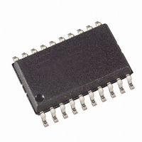
ATTINY2313-20SI Atmel, ATTINY2313-20SI Datasheet - Page 107

ATTINY2313-20SI
Manufacturer Part Number
ATTINY2313-20SI
Description
IC MCU AVR 2K FLASH 20SOIC
Manufacturer
Atmel
Series
AVR® ATtinyr
Specifications of ATTINY2313-20SI
Core Processor
AVR
Core Size
8-Bit
Speed
20MHz
Connectivity
SPI, UART/USART
Peripherals
Brown-out Detect/Reset, POR, PWM, WDT
Number Of I /o
18
Program Memory Size
2KB (1K x 16)
Program Memory Type
FLASH
Eeprom Size
128 x 8
Ram Size
128 x 8
Voltage - Supply (vcc/vdd)
2.7 V ~ 5.5 V
Oscillator Type
Internal
Operating Temperature
-40°C ~ 85°C
Package / Case
20-SOIC (7.5mm Width)
Lead Free Status / RoHS Status
Contains lead / RoHS non-compliant
Data Converters
-
Other names
ATTINY2313-24SI
ATTINY2313-24SI
ATTINY2313-24SI
Available stocks
Company
Part Number
Manufacturer
Quantity
Price
Company:
Part Number:
ATTINY2313-20SI
Manufacturer:
AT
Quantity:
95
Part Number:
ATTINY2313-20SI
Manufacturer:
RASTRONIC
Quantity:
20 000
- Current page: 107 of 226
- Download datasheet (4Mb)
Timer/Counter1
Control Register B –
TCCR1B
2543L–AVR–08/10
• Bit 7 – ICNC1: Input Capture Noise Canceler
Setting this bit (to one) activates the Input Capture Noise Canceler. When the noise canceler is
activated, the input from the Input Capture pin (ICP1) is filtered. The filter function requires four
successive equal valued samples of the ICP1 pin for changing its output. The Input Capture is
therefore delayed by four Oscillator cycles when the noise canceler is enabled.
• Bit 6 – ICES1: Input Capture Edge Select
This bit selects which edge on the Input Capture pin (ICP1) that is used to trigger a capture
event. When the ICES1 bit is written to zero, a falling (negative) edge is used as trigger, and
when the ICES1 bit is written to one, a rising (positive) edge will trigger the capture.
When a capture is triggered according to the ICES1 setting, the counter value is copied into the
Input Capture Register (ICR1). The event will also set the Input Capture Flag (ICF1), and this
can be used to cause an Input Capture Interrupt, if this interrupt is enabled.
When the ICR1 is used as TOP value (see description of the WGM13:0 bits located in the
TCCR1A and the TCCR1B Register), the ICP1 is disconnected and consequently the Input Cap-
ture function is disabled.
• Bit 5 – Reserved Bit
This bit is reserved for future use. For ensuring compatibility with future devices, this bit must be
written to zero when TCCR1B is written.
• Bit 4:3 – WGM13:2: Waveform Generation Mode
See TCCR1A Register description.
• Bit 2:0 – CS12:0: Clock Select
The three Clock Select bits select the clock source to be used by the Timer/Counter, see
49
Table 47. Clock Select Bit Description
If external pin modes are used for the Timer/Counter1, transitions on the T1 pin will clock the
counter even if the pin is configured as an output. This feature allows software control of the
counting.
Bit
Read/Write
Initial Value
CS12
and
0
0
0
0
1
1
1
1
Figure
CS11
0
0
1
1
0
0
1
1
ICNC1
50.
R/W
7
0
CS10
ICES1
0
1
0
1
0
1
0
1
R/W
6
0
Description
No clock source (Timer/Counter stopped).
clk
clk
clk
clk
clk
External clock source on T1 pin. Clock on falling edge.
External clock source on T1 pin. Clock on rising edge.
I/O
I/O
I/O
I/O
I/O
R
5
–
0
/1 (No prescaling)
/8 (From prescaler)
/64 (From prescaler)
/256 (From prescaler)
/1024 (From prescaler)
WGM13
R/W
4
0
WGM12
R/W
3
0
CS12
R/W
2
0
CS11
R/W
1
0
CS10
R/W
0
0
TCCR1B
Figure
107
Related parts for ATTINY2313-20SI
Image
Part Number
Description
Manufacturer
Datasheet
Request
R

Part Number:
Description:
IC, MCU, 8BIT, 2K FLASH, 20SOIC
Manufacturer:
Atmel
Datasheet:

Part Number:
Description:
IC, MCU, 8BIT, 2K FLASH, 20PDIP
Manufacturer:
Atmel
Datasheet:

Part Number:
Description:
IC, MCU, 8BIT, 8K FLASH, 20PDIP
Manufacturer:
Atmel
Datasheet:

Part Number:
Description:
IC, MCU, 8BIT, 8K FLASH, 20SOIC
Manufacturer:
Atmel
Datasheet:

Part Number:
Description:
DEV KIT FOR AVR/AVR32
Manufacturer:
Atmel
Datasheet:

Part Number:
Description:
INTERVAL AND WIPE/WASH WIPER CONTROL IC WITH DELAY
Manufacturer:
ATMEL Corporation
Datasheet:

Part Number:
Description:
Low-Voltage Voice-Switched IC for Hands-Free Operation
Manufacturer:
ATMEL Corporation
Datasheet:

Part Number:
Description:
MONOLITHIC INTEGRATED FEATUREPHONE CIRCUIT
Manufacturer:
ATMEL Corporation
Datasheet:

Part Number:
Description:
AM-FM Receiver IC U4255BM-M
Manufacturer:
ATMEL Corporation
Datasheet:

Part Number:
Description:
Monolithic Integrated Feature Phone Circuit
Manufacturer:
ATMEL Corporation
Datasheet:

Part Number:
Description:
Multistandard Video-IF and Quasi Parallel Sound Processing
Manufacturer:
ATMEL Corporation
Datasheet:

Part Number:
Description:
High-performance EE PLD
Manufacturer:
ATMEL Corporation
Datasheet:


