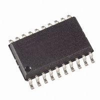
ATTINY2313-20SI Atmel, ATTINY2313-20SI Datasheet - Page 15

ATTINY2313-20SI
Manufacturer Part Number
ATTINY2313-20SI
Description
IC MCU AVR 2K FLASH 20SOIC
Manufacturer
Atmel
Series
AVR® ATtinyr
Specifications of ATTINY2313-20SI
Core Processor
AVR
Core Size
8-Bit
Speed
20MHz
Connectivity
SPI, UART/USART
Peripherals
Brown-out Detect/Reset, POR, PWM, WDT
Number Of I /o
18
Program Memory Size
2KB (1K x 16)
Program Memory Type
FLASH
Eeprom Size
128 x 8
Ram Size
128 x 8
Voltage - Supply (vcc/vdd)
2.7 V ~ 5.5 V
Oscillator Type
Internal
Operating Temperature
-40°C ~ 85°C
Package / Case
20-SOIC (7.5mm Width)
Lead Free Status / RoHS Status
Contains lead / RoHS non-compliant
Data Converters
-
Other names
ATTINY2313-24SI
ATTINY2313-24SI
ATTINY2313-24SI
Available stocks
Company
Part Number
Manufacturer
Quantity
Price
Company:
Part Number:
ATTINY2313-20SI
Manufacturer:
AT
Quantity:
95
Part Number:
ATTINY2313-20SI
Manufacturer:
RASTRONIC
Quantity:
20 000
- Current page: 15 of 226
- Download datasheet (4Mb)
SRAM Data
Memory
Data Memory Access
Times
2543L–AVR–08/10
Figure 9
The lower 224 data memory locations address both the Register File, the I/O memory, Extended
I/O memory, and the internal data SRAM. The first 32 locations address the Register File, the
next 64 location the standard I/O memory, and the next 128 locations address the internal data
SRAM.
The five different addressing modes for the data memory cover: Direct, Indirect with Displace-
ment, Indirect, Indirect with Pre-decrement, and Indirect with Post-increment. In the Register
File, registers R26 to R31 feature the indirect addressing pointer registers.
The direct addressing reaches the entire data space.
The Indirect with Displacement mode reaches 63 address locations from the base address given
by the Y- or Z-register.
When using register indirect addressing modes with automatic pre-decrement and post-incre-
ment, the address registers X, Y, and Z are decremented or incremented.
The 32 general purpose working registers, 64 I/O Registers, and the 128 bytes of internal data
SRAM in the ATtiny2313 are all accessible through all these addressing modes. The Register
File is described in
Figure 9. Data Memory Map
This section describes the general access timing concepts for internal memory access. The
internal data SRAM access is performed in two clk
shows how the ATtiny2313 SRAM Memory is organized.
“General Purpose Register File” on page
64 I/O Registers
Data Memory
Internal SRAM
32 Registers
(128 x 8)
0x00DF
0x0000 - 0x001F
0x0020 - 0x005F
0x0060
CPU
cycles as described in
9.
Figure
10.
15
Related parts for ATTINY2313-20SI
Image
Part Number
Description
Manufacturer
Datasheet
Request
R

Part Number:
Description:
IC, MCU, 8BIT, 2K FLASH, 20SOIC
Manufacturer:
Atmel
Datasheet:

Part Number:
Description:
IC, MCU, 8BIT, 2K FLASH, 20PDIP
Manufacturer:
Atmel
Datasheet:

Part Number:
Description:
IC, MCU, 8BIT, 8K FLASH, 20PDIP
Manufacturer:
Atmel
Datasheet:

Part Number:
Description:
IC, MCU, 8BIT, 8K FLASH, 20SOIC
Manufacturer:
Atmel
Datasheet:

Part Number:
Description:
DEV KIT FOR AVR/AVR32
Manufacturer:
Atmel
Datasheet:

Part Number:
Description:
INTERVAL AND WIPE/WASH WIPER CONTROL IC WITH DELAY
Manufacturer:
ATMEL Corporation
Datasheet:

Part Number:
Description:
Low-Voltage Voice-Switched IC for Hands-Free Operation
Manufacturer:
ATMEL Corporation
Datasheet:

Part Number:
Description:
MONOLITHIC INTEGRATED FEATUREPHONE CIRCUIT
Manufacturer:
ATMEL Corporation
Datasheet:

Part Number:
Description:
AM-FM Receiver IC U4255BM-M
Manufacturer:
ATMEL Corporation
Datasheet:

Part Number:
Description:
Monolithic Integrated Feature Phone Circuit
Manufacturer:
ATMEL Corporation
Datasheet:

Part Number:
Description:
Multistandard Video-IF and Quasi Parallel Sound Processing
Manufacturer:
ATMEL Corporation
Datasheet:

Part Number:
Description:
High-performance EE PLD
Manufacturer:
ATMEL Corporation
Datasheet:


