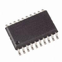
ATTINY2313-20SI Atmel, ATTINY2313-20SI Datasheet - Page 69

ATTINY2313-20SI
Manufacturer Part Number
ATTINY2313-20SI
Description
IC MCU AVR 2K FLASH 20SOIC
Manufacturer
Atmel
Series
AVR® ATtinyr
Specifications of ATTINY2313-20SI
Core Processor
AVR
Core Size
8-Bit
Speed
20MHz
Connectivity
SPI, UART/USART
Peripherals
Brown-out Detect/Reset, POR, PWM, WDT
Number Of I /o
18
Program Memory Size
2KB (1K x 16)
Program Memory Type
FLASH
Eeprom Size
128 x 8
Ram Size
128 x 8
Voltage - Supply (vcc/vdd)
2.7 V ~ 5.5 V
Oscillator Type
Internal
Operating Temperature
-40°C ~ 85°C
Package / Case
20-SOIC (7.5mm Width)
Lead Free Status / RoHS Status
Contains lead / RoHS non-compliant
Data Converters
-
Other names
ATTINY2313-24SI
ATTINY2313-24SI
ATTINY2313-24SI
Available stocks
Company
Part Number
Manufacturer
Quantity
Price
Company:
Part Number:
ATTINY2313-20SI
Manufacturer:
AT
Quantity:
95
Part Number:
ATTINY2313-20SI
Manufacturer:
RASTRONIC
Quantity:
20 000
- Current page: 69 of 226
- Download datasheet (4Mb)
Phase Correct PWM
Mode
2543L–AVR–08/10
The PWM frequency for the output can be calculated by the following equation:
The N variable represents the prescale factor (1, 8, 64, 256, or 1024).
The extreme values for the OCR0A Register represents special cases when generating a PWM
waveform output in the fast PWM mode. If the OCR0A is set equal to BOTTOM, the output will
be a narrow spike for each MAX+1 timer clock cycle. Setting the OCR0A equal to MAX will result
in a constantly high or low output (depending on the polarity of the output set by the COM0A1:0
bits.)
A frequency (with 50% duty cycle) waveform output in fast PWM mode can be achieved by set-
ting OC0x to toggle its logical level on each Compare Match (COM0x1:0 = 1). The waveform
generated will have a maximum frequency of f
feature is similar to the OC0A toggle in CTC mode, except the double buffer feature of the Out-
put Compare unit is enabled in the fast PWM mode.
The phase correct PWM mode (WGM02:0 = 1 or 5) provides a high resolution phase correct
PWM waveform generation option. The phase correct PWM mode is based on a dual-slope
operation. The counter counts repeatedly from BOTTOM to TOP and then from TOP to BOT-
TOM. TOP is defined as 0xFF when WGM2:0 = 1, and OCR0A when WGM2:0 = 5. In non-
inverting Compare Output mode, the Output Compare (OC0x) is cleared on the Compare Match
between TCNT0 and OCR0x while upcounting, and set on the Compare Match while down-
counting. In inverting Output Compare mode, the operation is inverted. The dual-slope operation
has lower maximum operation frequency than single slope operation. However, due to the sym-
metric feature of the dual-slope PWM modes, these modes are preferred for motor control
applications.
In phase correct PWM mode the counter is incremented until the counter value matches TOP.
When the counter reaches TOP, it changes the count direction. The TCNT0 value will be equal
to TOP for one timer clock cycle. The timing diagram for the phase correct PWM mode is shown
on
dual-slope operation. The diagram includes non-inverted and inverted PWM outputs. The small
horizontal line marks on the TCNT0 slopes represent Compare Matches between OCR0x and
TCNT0.
Figure
33. The TCNT0 value is in the timing diagram shown as a histogram for illustrating the
f
OCnxPWM
OC0
=
----------------- -
N 256
f
= f
clk_I/O
⋅
clk_I/O
/2 when OCR0A is set to zero. This
69
Related parts for ATTINY2313-20SI
Image
Part Number
Description
Manufacturer
Datasheet
Request
R

Part Number:
Description:
IC, MCU, 8BIT, 2K FLASH, 20SOIC
Manufacturer:
Atmel
Datasheet:

Part Number:
Description:
IC, MCU, 8BIT, 2K FLASH, 20PDIP
Manufacturer:
Atmel
Datasheet:

Part Number:
Description:
IC, MCU, 8BIT, 8K FLASH, 20PDIP
Manufacturer:
Atmel
Datasheet:

Part Number:
Description:
IC, MCU, 8BIT, 8K FLASH, 20SOIC
Manufacturer:
Atmel
Datasheet:

Part Number:
Description:
DEV KIT FOR AVR/AVR32
Manufacturer:
Atmel
Datasheet:

Part Number:
Description:
INTERVAL AND WIPE/WASH WIPER CONTROL IC WITH DELAY
Manufacturer:
ATMEL Corporation
Datasheet:

Part Number:
Description:
Low-Voltage Voice-Switched IC for Hands-Free Operation
Manufacturer:
ATMEL Corporation
Datasheet:

Part Number:
Description:
MONOLITHIC INTEGRATED FEATUREPHONE CIRCUIT
Manufacturer:
ATMEL Corporation
Datasheet:

Part Number:
Description:
AM-FM Receiver IC U4255BM-M
Manufacturer:
ATMEL Corporation
Datasheet:

Part Number:
Description:
Monolithic Integrated Feature Phone Circuit
Manufacturer:
ATMEL Corporation
Datasheet:

Part Number:
Description:
Multistandard Video-IF and Quasi Parallel Sound Processing
Manufacturer:
ATMEL Corporation
Datasheet:

Part Number:
Description:
High-performance EE PLD
Manufacturer:
ATMEL Corporation
Datasheet:


