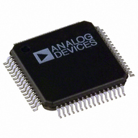
ADUC7024BST62-REEL Analog Devices Inc, ADUC7024BST62-REEL Datasheet - Page 28

ADUC7024BST62-REEL
Manufacturer Part Number
ADUC7024BST62-REEL
Description
IC MCU FLASH 62K W/ANLG 64-LQFP
Manufacturer
Analog Devices Inc
Series
MicroConverter® ADuC7xxxr
Datasheet
1.USB-I2CLIN-CONV-Z.pdf
(96 pages)
Specifications of ADUC7024BST62-REEL
Rohs Status
RoHS non-compliant
Design Resources
Sensing Low-g Acceleration Using ADXL345 Digital Accelerometer Connected to ADuC7024 (CN0133)
Core Processor
ARM7
Core Size
16/32-Bit
Speed
44MHz
Connectivity
EBI/EMI, I²C, SPI, UART/USART
Peripherals
PLA, PWM, PSM, Temp Sensor, WDT
Number Of I /o
30
Program Memory Size
62KB (62K x 8)
Program Memory Type
FLASH
Ram Size
8K x 8
Voltage - Supply (vcc/vdd)
2.7 V ~ 3.6 V
Data Converters
A/D 10x12b; D/A 2x12b
Oscillator Type
Internal
Operating Temperature
-40°C ~ 125°C
Package / Case
64-LQFP
Eeprom Size
-
Other names
ADUC7024BST62REEL
ADuC7019/20/21/22/24/25/26/27/28/29
Ball No.
D7
D8
E1
E2
E3
E4
E5
E6
E7
E8
F1
F2
F3
F4
F5
F6
F7
F8
G1
G2
G3
G4
G5
G6
G7
G8
H1
H2
H3
H4
H5
H6
H7
H8
Mnemonic
P1.6/SPM6/PLAI[6]
IOV
DAC3
DAC2
DAC1
P3.0/PWM0
P3.2/PWM1
P1.5/SPM5/PLAI[5]/IRQ3
P3.7/PWM
XCLKI
P4.6/PLAO[14]
TDI
DAC0s
P3.1/PWM0
P3.3/PWM1
RST
P0.7/ECLK/XCLK/SPM8/PLAO[4]
XCLKO
BM/P0.0/CMP
P4.7/PLAO[15]
TMS
TDO
P0.3/TRST/ADC
P3.4/PWM2
P3.5/PWM2
P2.0/SPM9/PLAO[5]/CONV
P0.6/T1/MRST/PLAO[3]
TCK
IOGND
IOV
LV
DGND
IRQ0/P0.4/PWM
IRQ1/P0.5/ADC
DD
DD
DD
SYNC
H
H
L
L
H
L
/PLAI[9]
/PLAI[11]
/PLAI[13]
/PLAI[8]
/PLAI[10]
/PLAI[12]
/PLAI[15]
OUT
BUSY
BUSY
TRIP
/PLAI[7]
/PLAO[2]
/PLAO[1]
START
Description
Serial Port Multiplexed. General-Purpose Input and Output Port 1.6/UART, SPI/Programmable
Logic Array Input Element 6.
3.3 V Supply for GPIO (see Table 78) and Input of the On-Chip Voltage Regulator.
DAC3 Voltage Output.
DAC2 Voltage Output.
DAC1 Voltage Output.
General-Purpose Input and Output Port 3.0/PWM Phase 0 High-Side Output/Programmable
Logic Array Input Element 8.
General-Purpose Input and Output Port 3.2/PWM Phase 1 High-Side Output/Programmable
Logic Array Input Element 10.
Serial Port Multiplexed. General-Purpose Input and Output Port 1.5/UART, SPI/Programmable
Logic Array Input Element 5/External Interrupt Request 3, Active High.
General-Purpose Input and Output Port 3.7/PWM Synchronization/Programmable Logic
Array Input Element 15.
Input to the Crystal Oscillator Inverter and Input to the Internal Clock Generator Circuits.
General-Purpose Input and Output Port 4.6/Programmable Logic Array Output Element 14.
JTAG Test Port Input, Test Data In. Debug and download access.
DAC0 Voltage Output.
General-Purpose Input and Output Port 3.1/PWM Phase 0 Low-Side Output/Programmable
Logic Array Input Element 9.
General-Purpose Input and Output Port 3.3/PWM Phase 1 Low-Side Output/Programmable
Logic Array Input Element 11.
Reset Input, Active Low.
Serial Port Multiplexed. General-Purpose Input and Output Port 0.7/Output for External
Clock Signal/Input to the Internal Clock Generator Circuits/UART/Programmable Logic Array
Output Element 4.
Output from the Crystal Oscillator Inverter.
Multifunction I/O Pin. Boot mode. The ADuC7028 enters UART download mode if BM is low
at reset and executes code if BM is pulled high at reset through a 1 kΩ resistor/General-
Purpose Input and Output Port 0.0/Voltage Comparator Output/Programmable Logic Array
Input Element 7.
General-Purpose Input and Output Port 4.7/Programmable Logic Array Output Element 15.
JTAG Test Port Input, Test Mode Select. Debug and download access.
JTAG Test Port Output, Test Data Out. Debug and download access.
General-Purpose Input and Output Port 0.3/JTAG Test Port Input, Test Reset/ADC
Output.
General-Purpose Input and Output Port 3.4/PWM Phase 2 High-Side Output/Programmable
Logic Array Input 12.
General-Purpose Input and Output Port 3.5/PWM Phase 2 Low-Side Output/Programmable
Logic Array Input Element 13.
Serial Port Multiplexed. General-Purpose Input and Output Port 2.0/UART/Programmable
Logic Array Output Element 5/Start Conversion Input Signal for ADC.
Multifunction Pin, Driven Low After Reset. General-Purpose Output Port 0.6/Timer1 Input/
Power-On Reset Output/Programmable Logic Array Output Element 3.
JTAG Test Port Input, Test Clock. Debug and download access.
Ground for GPIO (see Table 78). Typically connected to DGND.
3.3 V Supply for GPIO (see Table 78) and Input of the On-Chip Voltage Regulator.
2.6 V Output of the On-Chip Voltage Regulator. This output must be connected to a 0.47 μF
capacitor to DGND only.
Ground for Core Logic.
Multifunction I/O Pin. External Interrupt Request 0, Active High/General-Purpose Input and
Output Port 0.4/PWM Trip External Input/Programmable Logic Array Output Element 1.
Multifunction I/O Pin. External Interrupt Request 1, Active High/General-Purpose Input and
Output Port 0.5/ADC
Rev. C | Page 28 of 96
BUSY
Signal Output/Programmable Logic Array Output Element 2.
BUSY
Signal


