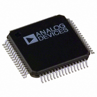
ADUC7024BST62-REEL Analog Devices Inc, ADUC7024BST62-REEL Datasheet - Page 37

ADUC7024BST62-REEL
Manufacturer Part Number
ADUC7024BST62-REEL
Description
IC MCU FLASH 62K W/ANLG 64-LQFP
Manufacturer
Analog Devices Inc
Series
MicroConverter® ADuC7xxxr
Datasheet
1.USB-I2CLIN-CONV-Z.pdf
(96 pages)
Specifications of ADUC7024BST62-REEL
Rohs Status
RoHS non-compliant
Design Resources
Sensing Low-g Acceleration Using ADXL345 Digital Accelerometer Connected to ADuC7024 (CN0133)
Core Processor
ARM7
Core Size
16/32-Bit
Speed
44MHz
Connectivity
EBI/EMI, I²C, SPI, UART/USART
Peripherals
PLA, PWM, PSM, Temp Sensor, WDT
Number Of I /o
30
Program Memory Size
62KB (62K x 8)
Program Memory Type
FLASH
Ram Size
8K x 8
Voltage - Supply (vcc/vdd)
2.7 V ~ 3.6 V
Data Converters
A/D 10x12b; D/A 2x12b
Oscillator Type
Internal
Operating Temperature
-40°C ~ 125°C
Package / Case
64-LQFP
Eeprom Size
-
Other names
ADUC7024BST62REEL
MEMORY ORGANIZATION
The ADuC7019/20/21/22/24/25/26/27/28/29 incorporate two
separate blocks of memory: 8 kB of SRAM and 64 kB of on-chip
Flash/EE memory. The 62 kB of on-chip Flash/EE memory is
available to the user, and the remaining 2 kB are reserved for
the factory-configured boot page. These two blocks are mapped
as shown in Figure 35.
Note that by default, after a reset, the Flash/EE memory is
mirrored at Address 0x00000000. It is possible to remap the
SRAM at Address 0x00000000 by clearing Bit 0 of the REMAP
MMR. This remap function is described in more detail in the
Flash/EE Memory section.
MEMORY ACCESS
The ARM7 core sees memory as a linear array of a 2
location where the different blocks of memory are mapped as
outlined in Figure 35.
The ADuC7019/20/21/22/24/25/26/27/28/29 memory organiza-
tions are configured in little endian format, which means that
the least significant byte is located in the lowest byte address,
and the most significant byte is in the highest byte address.
BIT 31
0xFFFF0000
0x40000000
0x30000000
0x20000000
0x10000000
0x00080000
0x00010000
0x00000000
BYTE 3
B
7
3
.
.
.
0x40000FFFF
0x30000FFFF
0x20000FFFF
0x10000FFFF
0xFFFFFFFF
0x0008FFFF
0x0000FFFF
0x00011FFF
Figure 35. Physical Memory Map
BYTE 2
Figure 36. Little Endian Format
A
6
2
.
.
.
32 BITS
BYTE 1
MMRs
RESERVED
EXTERNAL MEMORY REGION 3
RESERVED
EXTERNAL MEMORY REGION 2
RESERVED
EXTERNAL MEMORY REGION 1
RESERVED
EXTERNAL MEMORY REGION 0
RESERVED
FLASH/EE
RESERVED
SRAM
REMAPPABLE MEMORY SPACE
(FLASH/EE OR SRAM)
9
5
1
.
.
.
BYTE 0
8
4
0
.
.
.
BIT 0
0xFFFFFFFF
0x00000004
0x00000000
32
byte
Rev. C | Page 37 of 96
FLASH/EE MEMORY
The total 64 kB of Flash/EE memory is organized as 32 k × 16 bits;
31 k × 16 bits is user space and 1 k × 16 bits is reserved for the
on-chip kernel. The page size of this Flash/EE memory is 512 bytes.
Sixty-two kilobytes of Flash/EE memory are available to the
user as code and nonvolatile data memory. There is no
distinction between data and program because ARM code
shares the same space. The real width of the Flash/EE memory
is 16 bits, which means that in ARM mode (32-bit instruction),
two accesses to the Flash/EE are necessary for each instruction
fetch. It is therefore recommended to use thumb mode when
executing from Flash/EE memory for optimum access speed.
The maximum access speed for the Flash/EE memory is
41.78 MHz in thumb mode and 20.89 MHz in full ARM mode.
More details about Flash/EE access time are outlined in the
Execution Time from SRAM and Flash/EE section.
SRAM
Eight kilobytes of SRAM are available to the user, organized as
2 k × 32 bits, that is, two words. ARM code can run directly
from SRAM at 41.78 MHz, given that the SRAM array is
configured as a 32-bit wide memory array. More details about
SRAM access time are outlined in the Execution Time from
SRAM and Flash/EE section.
MEMORY MAPPED REGISTERS
The memory mapped register (MMR) space is mapped into the
upper two pages of the memory array and accessed by indirect
addressing through the ARM7 banked registers.
The MMR space provides an interface between the CPU and all
on-chip peripherals. All registers, except the core registers, reside
in the MMR area. All shaded locations shown in Figure 37 are
unoccupied or reserved locations and should not be accessed by
user software. Table 16 shows the full MMR memory map.
The access time for reading from or writing to an MMR
depends on the advanced microcontroller bus architecture
(AMBA) bus used to access the peripheral. The processor has
two AMBA buses: the advanced high performance bus (AHB)
used for system modules and the advanced peripheral bus
(APB) used for lower performance peripheral. Access to the
AHB is one cycle, and access to the APB is two cycles. All
peripherals on the ADuC7019/20/21/22/24/25/26/27/28/29 are
on the APB except the Flash/EE memory, the GPIOs (see Table
78), and the PWM.
ADuC7019/20/21/22/24/25/26/27/28/29


