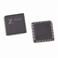
Z86D7308VSC1987 Zilog, Z86D7308VSC1987 Datasheet - Page 25

Z86D7308VSC1987
Manufacturer Part Number
Z86D7308VSC1987
Description
IC 32K OTP 3 VOLT 44-PLCC
Manufacturer
Zilog
Series
Z8® IRr
Datasheet
1.Z86D7308PSC1987.pdf
(92 pages)
Specifications of Z86D7308VSC1987
Core Processor
Z8
Core Size
8-Bit
Speed
8MHz
Peripherals
Brown-out Detect/Reset, LVD, POR, WDT
Number Of I /o
31
Program Memory Size
32KB (32K x 8)
Program Memory Type
OTP
Ram Size
236 x 8
Voltage - Supply (vcc/vdd)
2 V ~ 3.6 V
Oscillator Type
Internal
Operating Temperature
0°C ~ 70°C
Package / Case
44-LCC (J-Lead)
Lead Free Status / RoHS Status
Contains lead / RoHS non-compliant
Eeprom Size
-
Data Converters
-
Connectivity
-
PS019401-1102
XTAL1 Crystal 1 (Time-Based Input)
XTAL2 Crystal 2 (Time-Based Output)
R/W Read/Write (Output, Write Low)
R/RL (Input)
Port 0 (P07–P00)
Note:
This pin connects a parallel-resonant crystal, ceramic resonator, LC, or RC net-
work to the on-chip oscillator input. Additionally, an optional external single-phase
clock can be coded to the on-chip oscillator input.
This pin connects a parallel-resonant, crystal, ceramic resonant, LC, or RC net-
work to the on-chip oscillator output.
The R/W signal is Low when the CCP is writing to the external program or data
memory.
This pin, when connected to GND, disables the internal ROM and forces the
device to function as a ROMless Z8.
Port 0 is an 8-bit, bidirectional, CMOS-compatible port. These eight I/O lines are
configured under software control as a nibble I/O port or as an address port for
interfacing external memory. The output drivers are push-pull or open-drain con-
trolled by bit D2 in the PCON register.
For external memory references, Port 0 can provide address bits A11–A8 (lower
nibble) or A15–A8 (lower and upper nibble), depending on the required address
space. If the address range requires 12 bits or less, the upper nibble of Port 0 can
be programmed independently as I/O while the lower nibble is used for address-
ing. If one or both nibbles are needed for I/O operation, they must be configured
by writing to the Port 0 mode register. After a hardware reset, Port 0 is configured
as an input port.
Port 0 is set in the high-impedance mode (if selected as an address output), along
with Port 1 and the control signals AS, DS, and R/W through P3M bits D4 and D3
(see Figure 10).
A ROM mask option is available to program 0.4 V
P03. This option allows direct interface to mouse/trackball IR sensors.
When left unconnected or pulled high to V
normally as a Z8 ROM version.
P
R
E
L
I
M
I
N
A
40/44/48-Pin Low-Voltage IR OTP
R
CC
DD
, the part functions
Y
CMOS trip inputs on P00–
Z86D73
19


