Z8F0812SJ020EC Zilog, Z8F0812SJ020EC Datasheet - Page 11
Z8F0812SJ020EC
Manufacturer Part Number
Z8F0812SJ020EC
Description
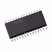
IC ENCORE MCU FLASH 8K 28SOIC
Manufacturer
Zilog
Series
Encore!® XP®r
Datasheet
1.Z8F08200100KIT.pdf
(264 pages)
Specifications of Z8F0812SJ020EC
Core Processor
Z8
Core Size
8-Bit
Speed
20MHz
Connectivity
I²C, IrDA, SPI, UART/USART
Peripherals
Brown-out Detect/Reset, POR, PWM, WDT
Number Of I /o
19
Program Memory Size
8KB (8K x 8)
Program Memory Type
FLASH
Ram Size
1K x 8
Voltage - Supply (vcc/vdd)
2.7 V ~ 3.6 V
Oscillator Type
Internal
Operating Temperature
-40°C ~ 105°C
Package / Case
28-SOIC (7.5mm Width)
Lead Free Status / RoHS Status
Contains lead / RoHS non-compliant
Eeprom Size
-
Data Converters
-
Other names
269-3228


PS022517-0508
Braces
The curly braces { }, indicate a single register or bus created by concatenating some com-
bination of smaller registers, buses, or individual bits.
•
Parentheses
The parentheses ( ), indicate an indirect register address lookup.
•
Parentheses/Bracket Combinations
The parentheses ( ), indicate an indirect register address lookup and the square brackets,
[ ], indicate a register or bus.
•
Use of the Words Set, Reset and Clear
The word set implies that a register bit or a condition contains a logical 1. The words reset
or clear imply that a register bit or a condition contains a logical 0. When either of these
terms is followed by a number, the word logical cannot be included; however, it is
implied.
Notation for Bits and Similar Registers
A field of bits within a register is designated as: Register[n:n].
•
Use of the Terms LSB, MSB, lsb, and msb
In this document, the terms LSB and MSB, when appearing in upper case, mean least
significant byte and most significant byte, respectively. The lowercase forms, lsb and msb,
mean least significant bit and most significant bit, respectively.
Use of Initial Uppercase Letters
Initial uppercase letters designate settings and conditions in general text.
•
•
Example: The 12-bit register address {
hexadecimal value (
(RP) and Working Register R1.
12-bit register, and R1[3:0] is the least significant nibble of the 12-bit register.
Example: (R1) is the memory location referenced by the address contained in the
Working Register R1.
Example: Assume PC[15:0] contains the value
contents of the memory location at address
Example: ADDR[15:0] refers to bits 15 through bit 0 of the Address.
Example 1: The receiver forces the SCL line to Low.
Example 2: The Master generates a STOP condition to abort the transfer.
0H
) and two 4-bit register values taken from the Register Pointer
0H
is the most significant nibble (4-bit value) of the
0H
, RP[7:4], R1[3:0]} is composed of a 4-bit
1234h
1234h
.
Z8 Encore! XP
. (PC [15:0]) then refers to the
Product Specification
®
F0822 Series
Introduction
xi
Related parts for Z8F0812SJ020EC
Image
Part Number
Description
Manufacturer
Datasheet
Request
R

Part Number:
Description:
Communication Controllers, ZILOG INTELLIGENT PERIPHERAL CONTROLLER (ZIP)
Manufacturer:
Zilog, Inc.
Datasheet:

Part Number:
Description:
KIT DEV FOR Z8 ENCORE 16K TO 64K
Manufacturer:
Zilog
Datasheet:

Part Number:
Description:
KIT DEV Z8 ENCORE XP 28-PIN
Manufacturer:
Zilog
Datasheet:

Part Number:
Description:
DEV KIT FOR Z8 ENCORE 8K/4K
Manufacturer:
Zilog
Datasheet:

Part Number:
Description:
KIT DEV Z8 ENCORE XP 28-PIN
Manufacturer:
Zilog
Datasheet:

Part Number:
Description:
DEV KIT FOR Z8 ENCORE 4K TO 8K
Manufacturer:
Zilog
Datasheet:
Part Number:
Description:
CMOS Z8 microcontroller. ROM 16 Kbytes, RAM 256 bytes, speed 16 MHz, 32 lines I/O, 3.0V to 5.5V
Manufacturer:
Zilog, Inc.
Datasheet:
Part Number:
Description:
Low-cost microcontroller. 512 bytes ROM, 61 bytes RAM, 8 MHz
Manufacturer:
Zilog, Inc.
Datasheet:
Part Number:
Description:
Z8 4K OTP Microcontroller
Manufacturer:
Zilog, Inc.
Datasheet:
Part Number:
Description:
CMOS SUPER8 ROMLESS MCU
Manufacturer:
Zilog, Inc.
Datasheet:
Part Number:
Description:
SL1866 CMOSZ8 OTP Microcontroller
Manufacturer:
Zilog, Inc.
Datasheet:
Part Number:
Description:
SL1866 CMOSZ8 OTP Microcontroller
Manufacturer:
Zilog, Inc.
Datasheet:
Part Number:
Description:
OTP (KB) = 1, RAM = 125, Speed = 12, I/O = 14, 8-bit Timers = 2, Comm Interfaces Other Features = Por, LV Protect, Voltage = 4.5-5.5V
Manufacturer:
Zilog, Inc.
Datasheet:
Part Number:
Description:
Manufacturer:
Zilog, Inc.
Datasheet: