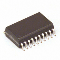
MC68HC908JB8JDW Freescale Semiconductor, MC68HC908JB8JDW Datasheet - Page 112

MC68HC908JB8JDW
Manufacturer Part Number
MC68HC908JB8JDW
Description
IC MCU 8K FLASH 3MHZ 20-SOIC
Manufacturer
Freescale Semiconductor
Series
HC08r
Datasheet
1.MC908JB8JDWE.pdf
(286 pages)
Specifications of MC68HC908JB8JDW
Core Processor
HC08
Core Size
8-Bit
Speed
3MHz
Connectivity
USB
Peripherals
LVD, POR, PWM
Number Of I /o
13
Program Memory Size
8KB (8K x 8)
Program Memory Type
FLASH
Ram Size
256 x 8
Voltage - Supply (vcc/vdd)
4 V ~ 5.5 V
Oscillator Type
Internal
Operating Temperature
0°C ~ 70°C
Package / Case
20-SOIC (7.5mm Width)
Lead Free Status / RoHS Status
Contains lead / RoHS non-compliant
Eeprom Size
-
Data Converters
-
Available stocks
Company
Part Number
Manufacturer
Quantity
Price
Part Number:
MC68HC908JB8JDW
Manufacturer:
MOTOROLA/摩托罗拉
Quantity:
20 000
Company:
Part Number:
MC68HC908JB8JDWE
Manufacturer:
VISHAY
Quantity:
6 700
Part Number:
MC68HC908JB8JDWE
Manufacturer:
FREESCALE
Quantity:
20 000
- Current page: 112 of 286
- Download datasheet (2Mb)
System Integration Module (SIM)
8.7.2 Stop Mode
Technical Data
112
NOTE:
NOTE:
In stop mode, the SIM counter is reset and the system clocks are
disabled. An interrupt request from a module can cause an exit from stop
mode. Stacking for interrupts begins after the selected stop recovery
time has elapsed. Reset or break also causes an exit from stop mode.
The SIM disables the oscillator signals (OSCOUT and OSCXCLK) in
stop mode, stopping the CPU and peripherals. Stop recovery time is
selectable using the SSREC bit in the configuration register (CONFIG).
If SSREC is set, stop recovery is reduced from the normal delay of 4096
OSCXCLK cycles down to 2048. This is ideal for applications using
canned oscillators that do not require long startup times from stop mode.
External crystal applications should use the full stop recovery time by
clearing the SSREC bit.
A break interrupt during stop mode sets the SIM break stop/wait bit
(SBSW) in the break status register (BSR).
The SIM counter is held in reset from the execution of the STOP
instruction until the beginning of stop recovery. It is then used to time the
recovery period.
To minimize stop current, all pins configured as inputs should be driven
to a logic 1 or logic 0.
CPUSTOP
NOTE: Previous data can be operand data or the STOP opcode, depending on the last
R/W
IAB
IDB
instruction.
System Integration Module (SIM)
STOP ADDR
Figure 8-16. Stop Mode Entry Timing
Figure 8-16
PREVIOUS DATA
MC68HC908JB8•MC68HC08JB8•MC68HC08JT8 — Rev. 2.3
STOP ADDR + 1
shows stop mode entry timing.
NEXT OPCODE
SAME
Freescale Semiconductor
SAME
SAME
SAME
Related parts for MC68HC908JB8JDW
Image
Part Number
Description
Manufacturer
Datasheet
Request
R
Part Number:
Description:
Manufacturer:
Freescale Semiconductor, Inc
Datasheet:
Part Number:
Description:
Manufacturer:
Freescale Semiconductor, Inc
Datasheet:
Part Number:
Description:
Manufacturer:
Freescale Semiconductor, Inc
Datasheet:
Part Number:
Description:
Manufacturer:
Freescale Semiconductor, Inc
Datasheet:
Part Number:
Description:
Manufacturer:
Freescale Semiconductor, Inc
Datasheet:
Part Number:
Description:
Manufacturer:
Freescale Semiconductor, Inc
Datasheet:
Part Number:
Description:
Manufacturer:
Freescale Semiconductor, Inc
Datasheet:
Part Number:
Description:
Manufacturer:
Freescale Semiconductor, Inc
Datasheet:
Part Number:
Description:
Manufacturer:
Freescale Semiconductor, Inc
Datasheet:
Part Number:
Description:
Manufacturer:
Freescale Semiconductor, Inc
Datasheet:
Part Number:
Description:
Manufacturer:
Freescale Semiconductor, Inc
Datasheet:
Part Number:
Description:
Manufacturer:
Freescale Semiconductor, Inc
Datasheet:
Part Number:
Description:
Manufacturer:
Freescale Semiconductor, Inc
Datasheet:
Part Number:
Description:
Manufacturer:
Freescale Semiconductor, Inc
Datasheet:
Part Number:
Description:
Manufacturer:
Freescale Semiconductor, Inc
Datasheet:


