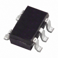
AD8061ARTZ-REEL7 Analog Devices Inc, AD8061ARTZ-REEL7 Datasheet

AD8061ARTZ-REEL7
Specifications of AD8061ARTZ-REEL7
Available stocks
Related parts for AD8061ARTZ-REEL7
AD8061ARTZ-REEL7 Summary of contents
Page 1
FEATURES Low cost Single (AD8061), dual (AD8062) Single with disable (AD8063) Rail-to-rail output swing Low offset voltage High speed 300 MHz, −3 dB bandwidth ( 650 V/μs slew rate 8.5 nV/√ ...
Page 2
AD8061/AD8062/AD8063 TABLE OF CONTENTS Features .............................................................................................. 1 Applications ....................................................................................... 1 Connection Diagrams ...................................................................... 1 General Description ......................................................................... 1 Revision History ............................................................................... 2 Specifications ..................................................................................... 3 Absolute Maximum Ratings ............................................................ 6 Maximum Power Dissipation ..................................................... 6 ESD Caution .................................................................................. 6 Typical ...
Page 3
SPECIFICATIONS T = 25° kΩ unless otherwise noted Table 1. Parameter DYNAMIC PERFORMANCE −3 dB Small Signal Bandwidth −3 dB Large Signal Bandwidth Bandwidth for ...
Page 4
AD8061/AD8062/AD8063 T = 25° kΩ unless otherwise noted Table 2. Parameter DYNAMIC PERFORMANCE –3 dB Small Signal Bandwidth –3 dB Large Signal Bandwidth Bandwidth for ...
Page 5
T = 25° 2 kΩ unless otherwise noted Table 3. Parameter DYNAMIC PERFORMANCE –3 dB Small Signal Bandwidth Bandwidth for 0.1 dB Flatness Slew Rate Settling ...
Page 6
AD8061/AD8062/AD8063 ABSOLUTE MAXIMUM RATINGS Table 4. Parameter Rating Supply Voltage Internal Power Dissipation 8-lead SOIC (R) 0.8 W 5-lead SOT-23 (RJ) 0.5 W 6-lead SOT-23 (RJ) 0.5 W 8-lead MSOP (RM) 0.6 W Input Voltage (Common-Mode) (−V ...
Page 7
TYPICAL PERFORMANCE CHARACTERISTICS 1.2 1.0 +V OUT +V @ +25°C OUT 0 –40°C OUT 0.6 –V @ –40°C OUT 0.4 0.2 –V @ +25°C OUT LOAD CURRENT (mA) Figure 7. Output ...
Page 8
AD8061/AD8062/AD8063 3 0 – –2 – –5 –9 – FREQUENCY (MHz) Figure 13. Large Signal Frequency Response 0 –0 –0 –0.3 –0.4 –0.5 ...
Page 9
1kΩ –50 2ND @ 10MHz – 10µF 1MΩ 0.1µF INPUT –70 50Ω TO 50Ω 1kΩ 1kΩ 3589A 1kΩ –80 2ND @ 500kHz –90 3RD ...
Page 10
AD8061/AD8062/AD8063 1400 FALLING EDGE 1200 V = ±4V S 1000 FALLING EDGE V = +5V S 800 600 400 RISING EDGE V S 200 0 0 0.5 1.0 1.5 2.0 OUTPUT STEP (V) Figure 25. Slew Rate vs. Output Step ...
Page 11
1kΩ – –20 –PSRR –30 –40 –50 +PSRR –60 –70 –80 –90 –100 0.01 0 FREQUENCY (MHz) Figure 31. ±PSRR vs. Frequency Delta –20 1kΩ ...
Page 12
AD8061/AD8062/AD8063 +0.1% –0.1% 1kΩ 50Ω 20ns/DIV Figure 37. Output Settling Time to 0. FALLING EDGE 40 35 RISING EDGE 0.5 1.0 1.5 OUTPUT VOLTAGE STEP Figure 38. Settling ...
Page 13
TIME (ns) Figure 43. 200 mV Step Response 1kΩ L 4.5V 2.5V 0.5V 1V/DIV Rev. ...
Page 14
AD8061/AD8062/AD8063 CIRCUIT DESCRIPTION The AD8061/AD8062/AD8063 family is comprised of high speed voltage feedback op amps. The high slew rate input stage is a true, single-supply topology, capable of sensing signals at or below the minus supply rail. The rail-to-rail output ...
Page 15
TO 3V STEP 2.8 2.1V TO 3.1V STEP 2.2V TO 3.2V STEP 2.6 2.3V TO 3.3V STEP 2.4 2.2 2 TIME (ns) Figure 47. Output Rising Edge for 1 ...
Page 16
AD8061/AD8062/AD8063 CAPACITIVE LOAD DRIVE The AD8061/AD8062/AD8063 family is optimized for bandwidth and speed, not for driving capacitive loads. Output capacitance creates a pole in the amplifier’s feedback path, leading to excessive peaking and potential oscillation. If dealing with load capacitance ...
Page 17
APPLICATIONS INFORMATION SINGLE-SUPPLY SYNC STRIPPER When a video signal contains synchronization pulses sometimes desirable to remove them prior to performing certain operations. In the case of analog-to-digital conversion, the sync pulses consume some of the dynamic range, so ...
Page 18
AD8061/AD8062/AD8063 MULTIPLEXER The AD8063 has a disable pin used to power down the ampli- fier to save power or to create a mux circuit. If two (or more) AD8063 outputs are connected together, and only one is enabled, then only ...
Page 19
OUTLINE DIMENSIONS 3.00 2.90 2. 3.00 1.70 2.80 1.60 2.60 1. 0.95 BSC 1.90 BSC 1.30 1.15 0.90 0.20 MAX 1.45 MAX 0.08 MIN 0.95 MIN 0.15 MAX SEATING 0.05 MIN 0.50 MAX PLANE 0.35 ...
Page 20
... AD8061ART-REEL −40°C to +85°C AD8061ART-REEL7 −40°C to +85°C AD8061ARTZ-R2 −40°C to +85°C AD8061ARTZ-REEL −40°C to +85°C AD8061ARTZ-REEL7 −40°C to +85°C AD8062AR −40°C to +85°C AD8062AR-REEL −40°C to +85°C AD8062AR-REEL7 −40°C to +85°C AD8062ARZ − ...


