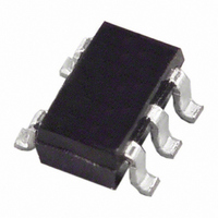
AD8061ARTZ-REEL7 Analog Devices Inc, AD8061ARTZ-REEL7 Datasheet - Page 14

AD8061ARTZ-REEL7
Manufacturer Part Number
AD8061ARTZ-REEL7
Description
IC OPAMP VF R-R LP 50MA SOT23-5
Manufacturer
Analog Devices Inc
Datasheet
1.AD8061ARTZ-REEL7.pdf
(20 pages)
Specifications of AD8061ARTZ-REEL7
Slew Rate
650 V/µs
Amplifier Type
Voltage Feedback
Number Of Circuits
1
Output Type
Rail-to-Rail
-3db Bandwidth
320MHz
Current - Input Bias
3.5µA
Voltage - Input Offset
1000µV
Current - Supply
6.8mA
Current - Output / Channel
50mA
Voltage - Supply, Single/dual (±)
2.7 V ~ 8 V, ±1.35 V ~ 4 V
Operating Temperature
-40°C ~ 85°C
Mounting Type
Surface Mount
Package / Case
SOT-23-5, SC-74A, SOT-25
Op Amp Type
Voltage Feedback
No. Of Amplifiers
1
Bandwidth
320MHz
Supply Voltage Range
2.7V To 8V
Amplifier Case Style
SOT-23
No. Of Pins
5
Rail/rail I/o Type
Rail to Rail Output
Number Of Elements
1
Common Mode Rejection Ratio
62dB
Input Offset Voltage
6@5VmV
Input Bias Current
9uA
Single Supply Voltage (typ)
5V
Dual Supply Voltage (typ)
Not RequiredV
Power Dissipation
500mW
Voltage Gain In Db
90dB
Power Supply Rejection Ratio
72dB
Power Supply Requirement
Single
Shut Down Feature
No
Single Supply Voltage (min)
2.7V
Single Supply Voltage (max)
8V
Dual Supply Voltage (min)
Not RequiredV
Dual Supply Voltage (max)
Not RequiredV
Operating Temp Range
-40C to 85C
Operating Temperature Classification
Industrial
Mounting
Surface Mount
Pin Count
5
Package Type
SOT-23
Lead Free Status / RoHS Status
Lead free / RoHS Compliant
Gain Bandwidth Product
-
Lead Free Status / Rohs Status
Compliant
Other names
AD8061ARTZ-REEL7
Available stocks
Company
Part Number
Manufacturer
Quantity
Price
Company:
Part Number:
AD8061ARTZ-REEL7
Manufacturer:
AD
Quantity:
3 000
Part Number:
AD8061ARTZ-REEL7
Manufacturer:
ADI/亚德诺
Quantity:
20 000
AD8061/AD8062/AD8063
CIRCUIT DESCRIPTION
The AD8061/AD8062/AD8063 family is comprised of high
speed voltage feedback op amps. The high slew rate input stage
is a true, single-supply topology, capable of sensing signals at or
below the minus supply rail. The rail-to-rail output stage can
pull within 30 mV of either supply rail when driving light loads
and within 0.3 V when driving 150 Ω. High speed perform-
ance is maintained at supply voltages as low as 2.7 V.
HEADROOM CONSIDERATIONS
These amplifiers are designed for use in low voltage systems.
To obtain optimum performance, it is useful to understand the
behavior of the amplifier as input and output signals approach
the amplifier’s headroom limits.
The AD8061/AD8062/AD8063 input common-mode voltage
range extends from the negative supply voltage (actually 200 mV
below this), or ground for single-supply operation, to within
1.8 V of the positive supply voltage. Thus, at a gain of 2, the
AD8061/AD8062/AD8063 can provide full rail-to-rail output
swing for supply voltage as low as 3.6 V, assuming the input
signal swings from −V
the AD8061/AD8062/AD8063 can provide a rail-to-rail output
range down to 2.7 V total supply voltage.
Exceeding the headroom limit is not a concern for any inverting
gain on any supply voltage, as long as the reference voltage at
the amplifier’s positive input lies within the amplifier’s input
common-mode range.
The input stage is the headroom limit for signals when the
amplifier is used in a gain of 1 for signals approaching the
positive rail. Figure 45 shows a typical offset voltage vs. input
common-mode voltage for the AD8061/AD8062/AD8063
amplifier on a 5 V supply. Accurate dc performance is main-
tained from approximately 200 mV below the minus supply
to within 1.8 V of the positive supply. For high speed signals,
however, there are other considerations. Figure 46 shows −3 dB
bandwidth vs. dc input voltage for a unity-gain follower. As
the common-mode voltage approaches the positive supply,
the amplifier holds together well, but the bandwidth begins to
drop at 1.9 V within +V
This manifests itself in increased distortion or settling time.
Figure 16 plots the distortion of a 1 V p-p signal with the
AD8061/AD8062/AD8063 amplifier used as a follower on
a 5 V supply vs. signal common-mode voltage. Distortion
performance is maintained until the input signal center voltage
gets beyond 2.5 V, as the peak of the input sine wave begins to
run into the upper common-mode voltage limit.
S
(or ground) to +V
S
.
S
/2. At a gain of 3,
Rev. G | Page 14 of 20
Higher frequency signals require more headroom than lower
frequencies to maintain distortion performance. Figure 47
illustrates how the rising edge settling time for the amplifier
configured as a unity-gain follower stretches out as the top of
a 1 V step input approaches and exceeds the specified input
common-mode voltage limit.
For signals approaching the minus supply and inverting gain
and high positive gain configurations, the headroom limit is
the output stage. The AD8061/AD8062/AD8063 amplifiers use
a common emitter style output stage. This output stage
maximizes the available output range, limited by the saturation
voltage of the output transistors. The saturation voltage
increases with the drive current the output transistor is required
to supply, due to the output transistors’ collector resistance. The
saturation voltage is estimated using the equation
where:
I
8 Ω is a typical value for the output transistors’ collector
resistance.
Figure 46. Unity-Gain Follower Bandwidth vs. Input Common Mode, V
O
is the output current.
V
SAT
–0.4
–0.8
–1.2
–1.6
–2.0
–2.4
–2.8
–3.2
–3.6
–4.0
–2
–4
–6
–8
2
0
–0.5
= 25 mV + I
0.1
Figure 45. V
0
1
0.5
OS
O
vs. Common-Mode Voltage, V
× 8 Ω
1.0
FREQUENCY (MHz)
10
1.5
V
CM
(V)
2.0
100
2.5
3.0
S
V
V
V
V
V
1k
= 5 V
CM
CM
CM
CM
CM
= 3.0
= 3.1
= 3.2
= 3.3
= 3.4
3.5
10k
4.0
S
= 5 V


