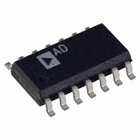
AD8279ARZ Analog Devices Inc, AD8279ARZ Datasheet - Page 16

AD8279ARZ
Manufacturer Part Number
AD8279ARZ
Description
IC AMP DIFF LP 14SOIC
Manufacturer
Analog Devices Inc
Datasheet
1.AD8279ARZ.pdf
(24 pages)
Specifications of AD8279ARZ
Amplifier Type
Differential
Number Of Circuits
2
Output Type
Rail-to-Rail
Slew Rate
1.4 V/µs
Gain Bandwidth Product
1MHz
Voltage - Input Offset
50µV
Current - Supply
300µA
Current - Output / Channel
15mA
Voltage - Supply, Single/dual (±)
2 V ~ 36 V, ±2 V ~ 18 V
Operating Temperature
-40°C ~ 85°C
Mounting Type
Surface Mount
Package / Case
14-SOIC (3.9mm Width), 14-SOL
No. Of Amplifiers
2
Input Offset Voltage
500µV
Bandwidth
1MHz
Supply Voltage Range
2V To 36V
Supply Current
200µA
Amplifier Case Style
SOIC
No. Of Pins
14
Rohs Compliant
Yes
Lead Free Status / RoHS Status
Lead free / RoHS Compliant
-3db Bandwidth
-
Current - Input Bias
-
Available stocks
Company
Part Number
Manufacturer
Quantity
Price
Company:
Part Number:
AD8279ARZ
Manufacturer:
Vishay
Quantity:
540
Part Number:
AD8279ARZ
Manufacturer:
ADI/亚德诺
Quantity:
20 000
AD8278/AD8279
THEORY OF OPERATION
CIRCUIT INFORMATION
Each channel of the AD8278 and AD8279 consists of a low power,
low noise op amp and four laser-trimmed on-chip resistors.
These resistors can be externally connected to make a variety
of amplifier configurations, including difference, noninverting,
and inverting configurations. Taking advantage of the integrated
resistors of the AD8278 and AD8279 provides the designer with
several benefits over a discrete design, including smaller size,
lower cost, and better ac and dc performance.
DC Performance
Much of the dc performance of op amp circuits depends on the
accuracy of the surrounding resistors. Using superposition to
analyze a typical difference amplifier circuit, as is shown in
Figure 49, the output voltage is found to be
This equation demonstrates that the gain accuracy and common-
mode rejection ratio of the AD8278 and AD8279 is determined
primarily by the matching of resistor ratios. Even a 0.1%
mismatch in one resistor degrades the CMRR to 69 dB for a
G = 2 difference amplifier.
The difference amplifier output voltage equation can be reduced to
as long as the following ratio of the resistors is tightly matched:
The resistors on the AD8278 and AD8279 are laser trimmed to
match accurately. As a result, the AD8278 and AD8279 provide
superior performance over a discrete solution, enabling better
CMRR, gain accuracy, and gain drift, even over a wide tempera-
ture range.
V
V
R2
R1
OUT
OUT
=
=
=
R4
R3
V
R4
R3
–IN
+IN
IN
+
(
Figure 48. Functional Block Diagram
V
2
3
⎛
⎜
⎜
⎝
IN
R1
+
40kΩ
40kΩ
R2
+
−
R2
V
IN
+VS
–VS
⎞
⎟
⎟
⎠
−
⎛ +
⎜
⎝
7
4
)
1
AD8278
20kΩ
20kΩ
R4
R3
⎞
⎟
⎠
−
V
5
6
1
IN
SENSE
OUT
REF
−
⎛
⎜
⎝
R4
R3
⎞
⎟
⎠
Rev. C | Page 16 of 24
AC Performance
Component sizes and trace lengths are much smaller in an IC
than on a PCB; therefore, the corresponding parasitic elements
are also smaller. This results in better ac performance of the
AD8278 and AD8279. For example, the positive and negative
input terminals of the AD8278 and AD8279 op amps are
intentionally not pinned out. By not connecting these nodes
to the traces on the PCB, their capacitance remains low and
balanced, resulting in improved loop stability and excellent
common-mode rejection over frequency.
DRIVING THE AD8278 AND AD8279
Care should be taken to drive the AD8278 and AD8279 with a
low impedance source, for example, another amplifier. Source
resistance of even a few kilohms (kΩ) can unbalance the resistor
ratios and, therefore, significantly degrade the gain accuracy and
common-mode rejection of the AD8278 and AD8279. Because all
configurations present several kilohms (kΩ) of input resistance,
the AD8278 and AD8279 do not require a high current drive
from the source and are easy to drive.
INPUT VOLTAGE RANGE
The AD8278 and AD8279 are able to measure input voltages
beyond the supply rails. The internal resistors divide down
the voltage before it reaches the internal op amp and provide
protection to the op amp inputs. Figure 49 shows an example
of how the voltage division works in a difference amplifier
configuration. For the AD8278 and AD8279 to measure correctly,
the input voltages at the input nodes of the internal op amp
must stay below 1.5 V of the positive supply rail and can exceed
the negative supply rail by 0.1 V. Refer to the Power Supplies
section for more details.
The AD8278 and AD8279 have integrated ESD diodes at the inputs
that provide overvoltage protection. This feature simplifies
system design by eliminating the need for additional external
protection circuitry and enables a more robust system.
The voltages at any of the inputs of the parts can safely range
from +V
supplies, input voltages can go as high as ±30 V. Care should be
taken to not exceed the +V
to avoid damaging the parts.
Figure 49. Voltage Division in the Difference Amplifier Configuration
S
− 40 V up to −V
V
V
IN–
IN+
R1 + R2
R2
R3
R1
(V
S
S
+ 40 V. For example, on ±10 V
R2
IN+
− 40 V to −V
)
R1 + R2
R2
R4
(V
IN+
S
)
+ 40 V input limits


