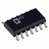
AD8279ARZ Analog Devices Inc, AD8279ARZ Datasheet - Page 4

AD8279ARZ
Manufacturer Part Number
AD8279ARZ
Description
IC AMP DIFF LP 14SOIC
Manufacturer
Analog Devices Inc
Datasheet
1.AD8279ARZ.pdf
(24 pages)
Specifications of AD8279ARZ
Amplifier Type
Differential
Number Of Circuits
2
Output Type
Rail-to-Rail
Slew Rate
1.4 V/µs
Gain Bandwidth Product
1MHz
Voltage - Input Offset
50µV
Current - Supply
300µA
Current - Output / Channel
15mA
Voltage - Supply, Single/dual (±)
2 V ~ 36 V, ±2 V ~ 18 V
Operating Temperature
-40°C ~ 85°C
Mounting Type
Surface Mount
Package / Case
14-SOIC (3.9mm Width), 14-SOL
No. Of Amplifiers
2
Input Offset Voltage
500µV
Bandwidth
1MHz
Supply Voltage Range
2V To 36V
Supply Current
200µA
Amplifier Case Style
SOIC
No. Of Pins
14
Rohs Compliant
Yes
Lead Free Status / RoHS Status
Lead free / RoHS Compliant
-3db Bandwidth
-
Current - Input Bias
-
Available stocks
Company
Part Number
Manufacturer
Quantity
Price
Company:
Part Number:
AD8279ARZ
Manufacturer:
Vishay
Quantity:
540
Part Number:
AD8279ARZ
Manufacturer:
ADI/亚德诺
Quantity:
20 000
AD8278/AD8279
V
otherwise noted.
Table 3.
Parameter
INPUT CHARACTERISTICS
DYNAMIC PERFORMANCE
GAIN
OUTPUT CHARACTERISTICS
NOISE
POWER SUPPLY
TEMPERATURE RANGE
1
2
3
4
5
6
7
Includes input bias and offset current errors, RTO (referred to output).
The input voltage range may also be limited by absolute maximum input voltage or by the output swing. See the
Internal resistors are trimmed to be ratio matched and have ±20% absolute accuracy.
Output voltage swing varies with supply voltage and temperature. See Figur
Includes amplifier voltage and current noise, as well as noise from internal resistors.
Supply current varies with supply voltage and temperature. See Figure
Unbalanced dual supplies can be used, such as −V
voltage.
S
System Offset
Common-Mode
Input Voltage Range
Impedance
Bandwidth
Slew Rate
Channel Separation
Settling Time to 0.01%
Settling Time to 0.001%
Gain Error
Gain Drift
Gain Nonlinearity
Output Voltage Swing
Short-Circuit Current
Capacitive Load Drive
Output Voltage Noise
AD8278 Supply Current
AD8279 Supply Current
Operating Voltage Range
Operating Range
= ±5 V to ±15 V, V
Over Temperature
vs. Power Supply
Average Temperature
Rejection Ratio (RTI)
Differential
Common Mode
Limit
Over Temperature
Over Temperature
5
Coefficient
3
6
1
2
REF
4
7
= 0 V, T
Conditions
T
V
T
V
R
f = 1 kHz
10 V step on output,
C
T
V
V
T
f = 0.1 Hz to 10 Hz
f = 1 kHz
T
T
A
A
A
A
A
A
S
S
S
L
OUT
S
= −40°C to +85°C
= ±5 V to ±18 V
= −40°C to +85°C
= ±15 V, V
= 0 Ω
= 100 pF
= −40°C to +85°C
= ±15 V, R
= −40°C to +85°C
= −40°C to +85°C
= −40°C to +85°C
A
= 20 V p-p
= 25°C, R
CM
L
= 10 kΩ,
S
= ±27 V,
= −0.5 V and +V
L
= 10 kΩ connected to ground, G = 2 difference amplifier configuration, unless
−1.5 (V
Min
86
1.1
−V
±2
−40
S
S
= +2 V. The positive supply rail must be at least 2 V above the negative supply and reference
+ 0.2
S
26
+ 0.1)
Rev. C | Page 4 of 24
and
e 22
Figure 28
Grade B
through
Typ
100
0.6
30
30
550
1.4
130
0.005
±15
350
2.8
90
300
for details.
Figure 25
+1.5 (V
Max
200
200
5
2
10
11
0.02
1
7
+V
95
200
250
350
400
±18
+125
S
− 0.2
S
− 1.5) −1.5 (V
for details.
G = 2
Min
80
1.1
−V
±2
−40
S
Input Voltage Range
+ 0.2
S
+ 0.1)
Grade A
Typ
100
2
30
30
550
1.4
130
0.01
±15
350
2.8
90
300
section for details.
+1.5 (V
Max
500
500
10
5
10
11
0.05
5
12
+V
95
200
250
350
400
±18
+125
S
− 0.2
S
− 1.5)
Unit
μV
μV
μV/V
μV/°C
dB
V
kΩ
kΩ
kHz
V/μs
dB
μs
μs
%
ppm/°C
ppm
V
mA
pF
μV p-p
nV/√Hz
μA
μA
μA
μA
V
°C


