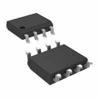
LM6171AIM/NOPB National Semiconductor, LM6171AIM/NOPB Datasheet - Page 18

LM6171AIM/NOPB
Manufacturer Part Number
LM6171AIM/NOPB
Description
IC AMP HI SPD LOW PWR V FB 8SOIC
Manufacturer
National Semiconductor
Series
PowerWise®, VIP™ IIIr
Datasheet
1.LM6171BIMNOPB.pdf
(21 pages)
Specifications of LM6171AIM/NOPB
Amplifier Type
Voltage Feedback
Number Of Circuits
1
Slew Rate
3600 V/µs
Gain Bandwidth Product
100MHz
-3db Bandwidth
160MHz
Current - Input Bias
1µA
Voltage - Input Offset
1500µV
Current - Supply
2.5mA
Current - Output / Channel
116mA
Voltage - Supply, Single/dual (±)
5.5 V ~ 34 V, ±2.75 V ~ 17 V
Operating Temperature
-40°C ~ 85°C
Mounting Type
Surface Mount
Package / Case
8-SOIC (3.9mm Width)
Lead Free Status / RoHS Status
Lead free / RoHS Compliant
Output Type
-
Other names
*LM6171AIM
*LM6171AIM/NOPB
LM6171AIM
*LM6171AIM/NOPB
LM6171AIM
www.national.com
Application Information
To minimize reflection, coaxial cable with matching charac-
teristic impedance to the signal source should be used. The
other end of the cable should be terminated with the same
value terminator or resistor. For the commonly used cables,
RG59 has 75Ω characteristic impedance, and RG58 has
50Ω characteristic impedance.
DRIVING CAPACITIVE LOADS
Amplifiers driving capacitive loads can oscillate or have ring-
ing at the output. To eliminate oscillation or reduce ringing,
an isolation resistor can be placed as shown below in Figure
5. The combination of the isolation resistor and the load
capacitor forms a pole to increase stablility by adding more
phase margin to the overall system. The desired perfor-
mance depends on the value of the isolation resistor; the
bigger the isolation resistor, the more damped the pulse
response becomes. For LM6171, a 50Ω isolation resistor is
recommended for initial evaluation. Figure 6 shows the
LM6171 driving a 200 pF load with the 50Ω isolation resistor.
POWER DISSIPATION
The maximum power allowed to dissipate in a device is
defined as:
Where P
FIGURE 6. The LM6171 Driving a 200 pF Load
T
T
θ
JA
J(max)
A
D
is the ambient temperature
FIGURE 5. Isolation Resistor Used
is the power dissipation in a device
is the thermal resistance of a particular package
with a 50Ω Isolation Resistor
is the maximum junction temperature
to Drive Capacitive Load
P
D
= (T
J(max)
− T
A
)/θ
JA
(Continued)
01233613
01233616
18
For example, for the LM6171 in a SO-8 package, the maxi-
mum power dissipation at 25˚C ambient temperature is
730 mW.
Thermal resistance, θ
die size, package size and package material. The smaller
the die size and package, the higher θ
DIP package has a lower thermal resistance (108˚C/W) than
that of 8-pin SO (172˚C/W). Therefore, for higher dissipation
capability, use an 8-pin DIP package.
The total power dissipated in a device can be calculated as:
P
connected at the output. P
device with a load connected at the output; it is not the power
dissipated by the load.
Furthermore,
For example, the total power dissipated by the LM6171 with
V
(one end tied to ground) is
APPLICATION CIRCUITS
Q
S
is the quiescent power dissipated in a device with no load
=
P
P
P
±
Q
L
D
15V and output voltage of 10V into 1 kΩ load resistor
=
= supply current x total supply voltage with no load
= P
= (2.5 mA) x (30V) + (10 mA) x (15V − 10V)
= 75 mW + 50 mW
= 125 mW
output current x (voltage difference between
supply voltage and output voltage of the same
supply)
Q
Fast Instrumentation Amplifier
+ P
L
JA
P
, depends on parameters such as
D
= P
L
is the power dissipated in the
Q
+ P
L
JA
becomes. The 8-pin
01233617


