LM6171AIM/NOPB National Semiconductor, LM6171AIM/NOPB Datasheet - Page 6

LM6171AIM/NOPB
Manufacturer Part Number
LM6171AIM/NOPB
Description
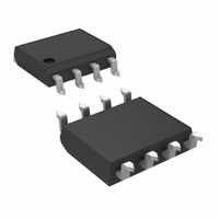
IC AMP HI SPD LOW PWR V FB 8SOIC
Manufacturer
National Semiconductor
Series
PowerWise®, VIP™ IIIr
Datasheet
1.LM6171BIMNOPB.pdf
(21 pages)
Specifications of LM6171AIM/NOPB
Amplifier Type
Voltage Feedback
Number Of Circuits
1
Slew Rate
3600 V/µs
Gain Bandwidth Product
100MHz
-3db Bandwidth
160MHz
Current - Input Bias
1µA
Voltage - Input Offset
1500µV
Current - Supply
2.5mA
Current - Output / Channel
116mA
Voltage - Supply, Single/dual (±)
5.5 V ~ 34 V, ±2.75 V ~ 17 V
Operating Temperature
-40°C ~ 85°C
Mounting Type
Surface Mount
Package / Case
8-SOIC (3.9mm Width)
Lead Free Status / RoHS Status
Lead free / RoHS Compliant
Output Type
-
Other names
*LM6171AIM
*LM6171AIM/NOPB
LM6171AIM
*LM6171AIM/NOPB
LM6171AIM
www.national.com
A
φ
e
i
Symbol
n
D
n
±
D
Unless otherwise specified, all limits guaranteed for T
limits apply at the temperature extremes
Note 1: Absolute Maximum Ratings indicate limits beyond which damage to the device may occur. Operating Ratings indicate conditions for which the device is
intended to be functional, but specific performance is not guaranteed. For guaranteed specifications and the test conditions, see the Electrical Characteristics.
Note 2: Human body model, 1.5 kΩ in series with 100 pF.
Note 3: Continuous short circuit operation at elevated ambient temperature can result in exceeding the maximum allowed junction temperature of 150˚C.
Note 4: The maximum power dissipation is a function of T
(T
Note 5: Typical Values represent the most likely parametric norm.
Note 6: All limits are guaranteed by testing or statistical analysis.
Note 7: Large signal voltage gain is the total output swing divided by the input signal required to produce that swing. For V
V
Note 8: The open loop output current is the output swing with the 100Ω load resistor divided by that resistor.
Note 9: Slew rate is the average of the rising and falling slew rates.
Note 10: Differential gain and phase are measured with A
OUT
J(max)
5V AC Electrical Characteristics
=
− T
±
1V.
Propagation Delay
Differential Gain (Note 10)
Differential Phase (Note 10)
Input-Referred
Voltage Noise
Input-Referred
Current Noise
A
)/θ
JA
. All numbers apply for packages soldered directly into a PC board.
Parameter
V
A
f = 1 kHz
f = 1 kHz
V
IN
V
J(max)
= +2, V
= −2
=
±
, θ
Conditions
1V, R
IN
J
JA
, and T
= 25˚C, V
= 1 V
(Continued)
L
PP
= 500Ω,
A
. The maximum allowable power dissipation at any ambient temperature is P
at 3.58 MHz and both input and output 75Ω terminated.
6
+
= +5V, V
(Note 5)
−
0.04
Typ
= −5V, V
0.7
11
8
1
CM
LM6171AI
(Note 6)
= 0V, and R
Limit
S
=
±
15V, V
LM6171BI
(Note 6)
L
Limit
= 1 kΩ. Boldface
OUT
=
±
5V. For V
Units
deg
S
ns
%
= +5V,
D
=


