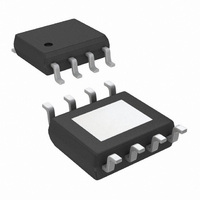
LME49724MR/NOPB National Semiconductor, LME49724MR/NOPB Datasheet - Page 14

LME49724MR/NOPB
Manufacturer Part Number
LME49724MR/NOPB
Description
IC AMP AUDIO MONO AB HIFI 8PSOP
Manufacturer
National Semiconductor
Datasheet
1.LME49724MRNOPB.pdf
(24 pages)
Specifications of LME49724MR/NOPB
Amplifier Type
Audio
Number Of Circuits
1
Output Type
Differential
Slew Rate
18 V/µs
Gain Bandwidth Product
50MHz
Current - Input Bias
60nA
Voltage - Input Offset
200µV
Current - Supply
10mA
Current - Output / Channel
80mA
Voltage - Supply, Single/dual (±)
5 V ~ 36 V, ±2.5 V ~ 18 V
Operating Temperature
-40°C ~ 85°C
Mounting Type
Surface Mount
Package / Case
8-PSOP
Lead Free Status / RoHS Status
Lead free / RoHS Compliant
-3db Bandwidth
-
www.national.com
Application Information
GENERAL OPERATION
The LME49724 is a fully differential amplifier with an integrat-
ed common-mode reference input (V
amplification provides increased noise immunity, high dy-
namic range, and reduced harmonic distortion products.
Differential amplifiers typically have high CMRR providing im-
proved immunity from noise. When input, output, and supply
line trace pairs are routed together, noise pick up is common
and easily rejected by the LME49724. CMRR performance is
directly proportional to the tolerance and matching of the gain
configuring resistors. With 0.1% tolerance resistors the worst
case CMRR performance will be about 60dB (20LOG
(0.001)).
A differential output has a higher dynamic range than a single-
ended output because of the doubling of output voltage. The
dynamic range is increased by 6dB as a result of the outputs
being equal in magnitude but opposite in phase. As an ex-
ample, a single-ended output with a 1V
1V
(2) = 6dB. Differential amplifiers are ideal for low voltage ap-
plications because of the increase in signal amplitude relative
to a single-ended amplifier and the resulting improvement in
SNR.
Differential amplifiers can also have reduced even order har-
monics, all conditions equal, when compared to a single-
ended amplifier. The differential output causes even harmon-
ics to cancel between the two inverted outputs leaving only
the odd harmonics. In practice even harmonics do not cancel
completely, however there still is a reduction in total harmonic
distortion.
OUTPUT COMMON-MODE VOLTAGE (V
The output common-mode voltage is the DC voltage on each
output. The output common-mode voltage is set by the
V
source. If no voltage is applied to the V
mon-mode output voltage will be set by the internal resistor
divider to the midpoint of the voltages on the V
pins. The input impedance of the V
V
V
capacitor. The V
the desired output common-mode voltage is ground refer-
ence. The value of the external capacitor has an effect on the
PSRR performance of the LME49724. With the V
bypassed with a low value capacitor, the PSRR performance
of the LME49724 will be reduced, especially at low audio fre-
quencies. For best PSRR performance, the V
be connected to stable, clean reference. Increasing the value
of the bypass capacitor on the V
PSRR performance.
ENABLE FUNCTION
The LME49724 can be placed into standby mode to reduce
system current consumption by driving the ENABLE pin be-
low V
on the ENABLE pin is above V
should not be left floating. For best performance under all
conditions, drive the ENABLE pin to the V
enter standby mode and to ground for active operation when
operating from split supplies. When operating from a single
OCM
OCM
OCM
PP
signals with a differential output. The increase is 20LOG
EE
pin can be driven up to V
pin should be bypassed to ground with a 0.1μF to 1μF
pin. The V
+ 1.75V. The LME49724 is active when the voltage
OCM
OCM
pin should be connected to ground when
pin can be driven by a low impedance
CC
EE
- 1.5V and V
+ 2.35V. The ENABLE pin
OCM
OCM
OCM
OCM
pin will also improve
PP
). Fully differential
OCM
pin is 50kΩ. The
signal will be two
pin, the DC com-
EE
OCM
EE
pin voltage to
pin)
OCM
+ 1.5V. The
CC
pin should
and V
pin only
EE
14
supply, drive the ENABLE pin to ground for standby mode and
to V
FULLY DIFFERENTIAL OPERATION
The LME49724 performs best in a fully differential configura-
tion. The circuit shown in Figure 2 is the typical fully differential
configuration.
The closed-loop gain is shown in Equation 1 below.
Where R
the lowest noise performance.
SINGLE-ENDED TO DIFFERENTIAL CONVERSION
For many applications, it is required to convert a single-ended
signal to a differential signal. The LME49724 can be used for
a high performance, simple single-to-differential converter.
Figure 3 shows the typical single-to-differential converter cir-
cuit configuration.
FIGURE 3. Single-Ended Input to Differential Output
CC
for active mode.
FIGURE 2. Fully Differential Configuration
F1
= R
F2
, R
A
V
i1
= R
= R
F
i2
/ R
. Using low value resistors will give
i
(V/V)
300442s0
300442r9
(1)


