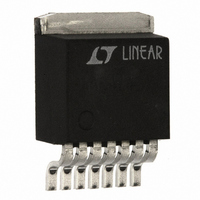
LT1206CR Linear Technology, LT1206CR Datasheet

LT1206CR
Specifications of LT1206CR
Available stocks
Related parts for LT1206CR
LT1206CR Summary of contents
Page 1
... LT1206 well suited to drive multiple cables in video systems. The LT1206 is manufactured on Linear Technology’s pro- prietary complementary bipolar process. L, LT, LTC, LTM, Linear Technology and the Linear logo are registered trademarks of Linear Technology Corporation. All other trademarks are the property of their respective owners ±15V ...
Page 2
... LTC1206CN8 LTC1206CN8#TR LT1206CS8** LT1206CS8#TR † LT1206CR LT1206CR#TR † LT1206CT7 LT1206CT7#TR Consult LTC Marketing for parts specified with wider operating temperature ranges. *The temperature grade is identified by a label on the shipping container. **Ground shutdown pin for normal operation. For more information on lead free part marking, go to: ...
Page 3
T SYMBOL PARAMETER V Input Offset Voltage OS Input Offset Voltage Drift + I Noninverting Input Current IN – I Inverting Input Current IN e Input Noise Voltage Density n +i Input ...
Page 4
LT1206 sMall-signal banDwiDTh I = 20mA Typical, Peaking ≤ 0.1dB ±5V 0Ω S S/D –1 150 562 562 30 649 649 10 732 732 1 150 619 ...
Page 5
Typical perForMance characTerisTics Bandwidth vs Supply Voltage 100 PEAKING ≤ 0.5dB PEAKING ≤ 5dB 100 470 560 680 ...
Page 6
LT1206 Typical perForMance characTerisTics Supply Current vs Supply Voltage S –40° 25° 85° 125° ...
Page 7
Typical perForMance characTerisTics Output Impedance vs Frequency 100 V = ±15V 0mA 121k S 0Ω S/D 1 0.1 0.01 100k 1M 10M 100M FREQUENCY (Hz) 1206 G19 3rd Order Intercept vs ...
Page 8
LT1206 siMpliFieD scheMaTic TO ALL CURRENT SOURCES Q18 Q17 1.25k SHUTDOWN applicaTions inForMaTion The LT1206 is a current feedback amplifier with high output current drive capability. The device is stable with large capacitive loads and can easily supply the high ...
Page 9
V = ±15V 1.2k F COMPENSATION COMPENSATION –2 F COMPENSATION –4 –6 – FREQUENCY (MHz) Figure 1 is ...
Page 10
LT1206 applicaTions inForMaTion For applications where the full bandwidth of the amplifier is not required, the quiescent current of the device may be reduced by connecting a resistor from the shutdown pin to ground. The quiescent current will be approximately ...
Page 11
R = 750Ω 20ns/DIV 50Ω L Figure 5c. Large-Signal Response, A When the LT1206 is used to drive capacitive loads, the available output current can limit the overall slew rate. In the fastest configuration, the ...
Page 12
LT1206 applicaTions inForMaTion power plane layer either inside or on the opposite side of the board. Although the actual thermal resistance of the PCB material is high, the length/area ratio of the thermal resistance between the layer is small. Copper ...
Page 13
Precision ×10 Hi Current Amplifier + V IN LT1097 – 500pF 330 OUTPUT OFFSET: < 500µV 1k SLEW RATE: 2V/µs BANDWIDTH: 4MHz STABLE WITH C < 10nF L Low Noise ×10 Buffered Line Driver 15V 1µF 15V 1µF ...
Page 14
LT1206 package DescripTion .300 – .325 (7.620 – 8.255) .008 – .015 (0.203 – 0.381) +.035 .325 –.015 ( ) +0.889 8.255 –0.381 NOTE: 1. DIMENSIONS ARE MILLIMETERS *THESE DIMENSIONS DO NOT INCLUDE MOLD FLASH OR PROTRUSIONS. MOLD FLASH OR ...
Page 15
DescripTion .060 .256 (1.524) (6.502) .060 .183 (1.524) (4.648) .075 (1.905) .300 (7.620) BOTTOM VIEW OF DD PAK HATCHED AREA IS SOLDER PLATED COPPER HEAT SINK .420 .050 RECOMMENDED SOLDER PAD LAYOUT NOTE: 1. DIMENSIONS IN INCH/(MILLIMETER) 2. DRAWING ...
Page 16
LT1206 package DescripTion .050 BSC .245 MIN .030 ±.005 TYP RECOMMENDED SOLDER PAD LAYOUT .010 – .020 (0.254 – 0.508) .008 – .010 (0.203 – 0.254) NOTE: 1. DIMENSIONS IN 2. DRAWING NOT TO SCALE 3. THESE DIMENSIONS DO NOT ...
Page 17
... Updated note on Table 2 in the Applications Information section. Information furnished by Linear Technology Corporation is believed to be accurate and reliable. However, no responsibility is assumed for its use. Linear Technology Corporation makes no representa- tion that the interconnection of its circuits as described herein will not infringe on existing patent rights. ...
Page 18
... High Power, High Speed Buffer Adjustable Supply Current, Shutdown Adjustable Supply Current, Shutdown 0.1dB Gain Flatness to 100MHz S6 Version Features Programmable Supply Current High Speed, Low Noise, Low Distortion, Low Offset www.linear.com ● 1206fb LT 0311 REV B • PRINTED IN USA LINEAR TECHNOLOGY CORPORATION 1993 ...


