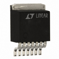
LT1206CR Linear Technology, LT1206CR Datasheet - Page 8

LT1206CR
Manufacturer Part Number
LT1206CR
Description
IC CURRNT FEEDBCK AMP 250MA 7-DD
Manufacturer
Linear Technology
Datasheet
1.LT1206CN8PBF.pdf
(18 pages)
Specifications of LT1206CR
Amplifier Type
Current Feedback
Number Of Circuits
1
Slew Rate
900 V/µs
-3db Bandwidth
60MHz
Current - Input Bias
10µA
Voltage - Input Offset
3000µV
Current - Supply
20mA
Current - Output / Channel
1.2A
Voltage - Supply, Single/dual (±)
10 V ~ 30 V, ±5 V ~ 15 V
Operating Temperature
0°C ~ 70°C
Mounting Type
Surface Mount
Package / Case
TO-263-7, D²Pak (7 leads + Tab), TO-263CA
Lead Free Status / RoHS Status
Contains lead / RoHS non-compliant
Output Type
-
Gain Bandwidth Product
-
Available stocks
Company
Part Number
Manufacturer
Quantity
Price
Company:
Part Number:
LT1206CR#PBF
Manufacturer:
AD
Quantity:
979
Part Number:
LT1206CR#PBF
Manufacturer:
LINEAR/凌特
Quantity:
20 000
Part Number:
LT1206CR#TRPBF
Manufacturer:
LINEAR/凌特
Quantity:
20 000
Company:
Part Number:
LT1206CR/CT7
Manufacturer:
LT
Quantity:
5 510
Company:
Part Number:
LT1206CR/CT7
Manufacturer:
HITACHI
Quantity:
5 510
LT1206
siMpliFieD scheMaTic
applicaTions inForMaTion
The LT1206 is a current feedback amplifier with high output
current drive capability. The device is stable with large
capacitive loads and can easily supply the high currents
required by capacitive loads. The amplifier will drive low
impedance loads such as cables with excellent linearity
at high frequencies.
Feedback Resistor Selection
The optimum value for the feedback resistors is a function
of the operating conditions of the device, the load imped-
ance and the desired flatness of response. The Typical AC
Performance tables give the values which result in the
highest 0.1dB and 0.5dB bandwidths for various resistive
loads and operating conditions. If this level of flatness is
not required, a higher bandwidth can be obtained by use
of a lower feedback resistor. The characteristic curves of
Bandwidth vs Supply Voltage indicate feedback resistors
for peaking up to 5dB. These curves use a solid line when
the response has less than 0.5dB of peaking and a dashed
8
Q17
SHUTDOWN
CURRENT
SOURCES
TO ALL
Q18
1.25k
+IN
V
V
Q1
Q3
–
+
Q2
Q4
–IN
Q5
Q7
line when the response has 0.5dB to 5dB of peaking. The
curves stop where the response has more than 5dB of
peaking.
For resistive loads, the COMP pin should be left open (see
section on capacitive loads).
Capacitive Loads
The LT1206 includes an optional compensation network
for driving capacitive loads. This network eliminates most
of the output stage peaking associated with capacitive
loads, allowing the frequency response to be flattened.
Figure 1 shows the effect of the network on a 200pF load.
Without the optional compensation, there is a 5dB peak
at 40MHz caused by the effect of the capacitance on the
output stage. Adding a 0.01µF bypass capacitor between the
output and the COMP pins connects the compensation and
completely eliminates the peaking. A lower value feedback
resistor can now be used, resulting in a response which
Q6
Q8
C
C
V
V
Q9
Q12
–
+
R
D2
D1
C
Q15
Q16
50Ω
COMP
Q13
Q10
Q11
Q14
1206 SS
V
OUTPUT
V
–
+
1206fb


