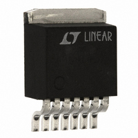
LT1206CR Linear Technology, LT1206CR Datasheet - Page 11

LT1206CR
Manufacturer Part Number
LT1206CR
Description
IC CURRNT FEEDBCK AMP 250MA 7-DD
Manufacturer
Linear Technology
Datasheet
1.LT1206CN8PBF.pdf
(18 pages)
Specifications of LT1206CR
Amplifier Type
Current Feedback
Number Of Circuits
1
Slew Rate
900 V/µs
-3db Bandwidth
60MHz
Current - Input Bias
10µA
Voltage - Input Offset
3000µV
Current - Supply
20mA
Current - Output / Channel
1.2A
Voltage - Supply, Single/dual (±)
10 V ~ 30 V, ±5 V ~ 15 V
Operating Temperature
0°C ~ 70°C
Mounting Type
Surface Mount
Package / Case
TO-263-7, D²Pak (7 leads + Tab), TO-263CA
Lead Free Status / RoHS Status
Contains lead / RoHS non-compliant
Output Type
-
Gain Bandwidth Product
-
Available stocks
Company
Part Number
Manufacturer
Quantity
Price
Company:
Part Number:
LT1206CR#PBF
Manufacturer:
AD
Quantity:
979
Part Number:
LT1206CR#PBF
Manufacturer:
LINEAR/凌特
Quantity:
20 000
Part Number:
LT1206CR#TRPBF
Manufacturer:
LINEAR/凌特
Quantity:
20 000
Company:
Part Number:
LT1206CR/CT7
Manufacturer:
LT
Quantity:
5 510
Company:
Part Number:
LT1206CR/CT7
Manufacturer:
HITACHI
Quantity:
5 510
applicaTions inForMaTion
When the LT1206 is used to drive capacitive loads, the
available output current can limit the overall slew rate. In
the fastest configuration, the LT1206 is capable of a slew
rate of over 1V/ns. The current required to slew a capaci-
tor at this rate is 1mA per picofarad of capacitance, so
10,000pF would require 10A! The photo (Figure 6) shows
the large signal behavior with C
is about 60V/µs, determined by the current limit of 600mA.
Differential Input Signal Swing
The differential input swing is limited to about ± 6V by
an ESD protection device connected between the inputs.
In normal operation, the differential voltage between the
input pins is small, so this clamp has no effect; however,
in the shutdown mode the differential swing can be the
same as the input swing. The clamp voltage will then set
Figure 6. Large-Signal Response, C
R
R
V
R
R
F
L
S
L
L
= 750Ω
= 50Ω
= ±15V
= R
= ∞
Figure 5c. Large-Signal Response, A
G
= 3k
500ns/DIV
20ns/DIV
L
= 10,000pF . The slew rate
L
= 10,000pF
V
= 2
1206 F05c
1206 G06
the maximum allowable input voltage. To allow for some
margin, it is recommended that the input signal be less
than ±5V when the device is shut down.
Capacitance on the Inverting Input
Current feedback amplifiers require resistive feedback from
the output to the inverting input for stable operation. Take
care to minimize the stray capacitance between the output
and the inverting input. Capacitance on the inverting input
to ground will cause peaking in the frequency response
(and overshoot in the transient response), but it does not
degrade the stability of the amplifier.
Power Supplies
The LT1206 will operate from single or split supplies from
± 5V (10V total) to ±15V (30V total). It is not necessary to
use equal value split supplies, however the offset voltage
and inverting input bias current will change. The offset
voltage changes about 500µV per volt of supply mismatch.
The inverting bias current can change as much as 5µA per
volt of supply mismatch, though typically the change is
less than 0.5µA per volt.
Thermal Considerations
The LT1206 contains a thermal shutdown feature which
protects against excessive internal (junction) temperature.
If the junction temperature of the device exceeds the pro-
tection threshold, the device will begin cycling between
normal operation and an off state. The cycling is not
harmful to the part. The thermal cycling occurs at a slow
rate, typically 10ms to several seconds, which depends
on the power dissipation and the thermal time constants
of the package and heat sinking. Raising the ambient
temperature until the device begins thermal shutdown
gives a good indication of how much margin there is in
the thermal design.
For surface mount devices heat sinking is accomplished
by using the heat spreading capabilities of the PC board
and its copper traces. Experiments have shown that the
heat spreading copper layer does not need to be electri-
cally connected to the tab of the device. The PCB material
can be very effective at transmitting heat between the pad
area attached to the tab of the device, and a ground or
LT1206
11
1206fb


