AD841JNZ Analog Devices Inc, AD841JNZ Datasheet - Page 2
AD841JNZ
Manufacturer Part Number
AD841JNZ
Description
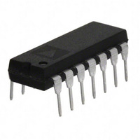
IC OPAMP GP 40MHZ 50MA 14DIP
Manufacturer
Analog Devices Inc
Datasheet
1.AD841JNZ.pdf
(8 pages)
Specifications of AD841JNZ
Slew Rate
300 V/µs
Amplifier Type
General Purpose
Number Of Circuits
1
Gain Bandwidth Product
40MHz
Current - Input Bias
3.5µA
Voltage - Input Offset
800µV
Current - Supply
11mA
Current - Output / Channel
50mA
Voltage - Supply, Single/dual (±)
±5 V ~ 18 V
Operating Temperature
0°C ~ 75°C
Mounting Type
Through Hole
Package / Case
14-DIP (0.300", 7.62mm)
Op Amp Type
Unity Gain Stable
No. Of Amplifiers
1
Bandwidth
40MHz
Supply Voltage Range
± 5V To ± 18V
Amplifier Case Style
DIP
No. Of Pins
14
Lead Free Status / RoHS Status
Lead free / RoHS Compliant
Output Type
-
-3db Bandwidth
-
Lead Free Status / RoHS Status
Lead free / RoHS Compliant, Lead free / RoHS Compliant
Available stocks
Company
Part Number
Manufacturer
Quantity
Price


AD841–SPECIFICATIONS
Model
INPUT OFFSET VOLTAGE
INPUT BIAS CURRENT
INPUT CHARACTERISTICS
INPUT VOLTAGE RANGE
INPUT VOLTAGE NOISE
OPEN-LOOP GAIN
OUTPUT CHARACTERISTICS
OUTPUT RESISTANCE
FREQUENCY RESPONSE
OVERDRIVE RECOVERY
DIFFERENTIAL GAIN
POWER SUPPLY
TEMPERATURE RANGE
PACKAGE OPTIONS
NOTES
1
2
3
3
4
All min and max specifications are guaranteed. Specifications shown in boldface are tested on all production units.
Specifications subject to change without notice.
Standard Military Drawing Available: 5962-89641012A – (SE/883B); 5962-8964101CA – (SQ/883B).
Input offset voltage specifications are guaranteed after 5 minutes at T
Full power bandwidth = Slew Rate/2
Refer to Figure 19.
“S” grade T
Offset Drift
Input Offset Current
Input Resistance
Input Capacitance
Common Mode
Common-Mode Rejection
Wideband Noise
Voltage
Current
Unity Gain Bandwidth
Full Power Bandwidth
Rise Time
Overshoot
Slew Rate
Settling Time – 10 V Step
Differential Phase
Rated Performance
Operating Range
Quiescent Current
Power Supply Rejection Ratio
Rated Performance
LCC (E-20A)
Cerdip (Q-14)
Plastic (N-14)
TO-8 (H-12)
Chips
MIN
4
4
4
–T
MAX
specifications are tested with automatic test equipment at T
5
3
2
V
PEAK
Conditions
T
T
T
Differential Mode
V
T
f = 1 kHz
10 Hz to 10 MHz
V
R
T
R
T
V
Open Loop
V
V
R
A
A
A
A
to 0.1%
to 0.01%
–Overdrive
+Overdrive
f = 4.4 MHz
f = 4.4 MHz
T
V
T
CM
O
LOAD
LOAD
OUT
OUT
O
LOAD
V
V
V
V
S
MIN
MIN
MIN
MIN
MIN
MIN
MIN
MIN
= 5 V to 18 V
= –1
= –1
= –1
= –1
= 10 V
= 20 V p-p
.
= 10 V
–T
–T
–T
–T
–T
–T
–T
–T
= 10 V
= 90 mV p-p
MAX
MAX
MAX
MAX
MAX
MAX
MAX
MAX
500
500
500
(@ +25 C and
Min
86
80
25
12
50
3.1
200
86
80
0
AD841J CHIPS
10
5
10
A
AD841JQ
AD841JN
AD841JH
= +25 C.
AD841J
Typ
0.8
35
3.5
0.1
200
2
12
100
15
47
45
5
40
4.7
10
10
300
90
110
200
700
0.03
0.022
11
100
15
–2–
15 V dc, unless otherwise noted)
A
= –55 C and T
Max
2.0
5.0
8
10
0.4
0.5
12
14
+75
18
103
100
25
20
50
3.1
200
90
86
0
Min
10
5
10
A
AD841KQ
AD841KN
AD841KH
AD841K
= +125 C.
0.5
35
3.5
0.1
200
2
12
109
15
47
45
5
40
4.7
10
10
300
00
110
200
700
0.03
0.022
11
100
Typ
15
1.0
3.3
5
6
0.2
0.3
14
+75
Max
12
18
86
80
25
12
50
3.1
200
86
80
–55
AD841SE, AD841SE/883B
AD841SQ, AD841SQ/883B
AD841SH, AD841SH/883B
Min
10
5
10
AD841S CHIPS
AD841S
0.5
35
3.5
0.1
2
12
110
15
47
45
5
4.7
90
700
0.03
0.022
100
200
40
10
10
300
110
200
11
Typ
15
1
Max
2.0
5.5
8
12
0.4
0.6
12
16
+125
18
Units
mV
mV
pF
V
dB
dB
nV/ Hz
V/mV
V/mV
V
mA
MHz
ns
%
ns
ns
ns
%
Degree
V
V
mA
mA
dB
dB
REV. B
k
MHz
V/ s
ns
C
V/ C
A
A
A
A
V rms
Related parts for AD841JNZ
Image
Part Number
Description
Manufacturer
Datasheet
Request
R

Part Number:
Description:
±1.7g Dual-Axis IMEMS Accelerometer Evaluation Board
Manufacturer:
Analog Devices Inc
Datasheet:

Part Number:
Description:
Inertial Sensor Evaluation System
Manufacturer:
Analog Devices Inc
Datasheet:
Part Number:
Description:
Manufacturer:
Analog Devices Inc
Datasheet:
Part Number:
Description:
Manufacturer:
Analog Devices Inc
Datasheet:
Part Number:
Description:
Manufacturer:
Analog Devices Inc
Datasheet:
Part Number:
Description:
Manufacturer:
Analog Devices Inc
Datasheet:
Part Number:
Description:
Manufacturer:
Analog Devices Inc
Datasheet:
Part Number:
Description:
Manufacturer:
Analog Devices Inc
Datasheet:
Part Number:
Description:
Manufacturer:
Analog Devices Inc
Datasheet:
Part Number:
Description:
Manufacturer:
Analog Devices Inc
Datasheet:
Part Number:
Description:
Manufacturer:
Analog Devices Inc
Datasheet:
Part Number:
Description:
Manufacturer:
Analog Devices Inc
Datasheet:
Part Number:
Description:
Manufacturer:
Analog Devices Inc
Datasheet: