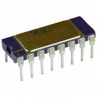
AD524CD Analog Devices Inc, AD524CD Datasheet - Page 19

AD524CD
Manufacturer Part Number
AD524CD
Description
IC AMP INST 1MHZ PREC LN 16CDIP
Manufacturer
Analog Devices Inc
Type
Precisionr
Specifications of AD524CD
Slew Rate
5 V/µs
Rohs Status
RoHS non-compliant
Amplifier Type
Instrumentation
Number Of Circuits
1
Gain Bandwidth Product
1MHz
-3db Bandwidth
1MHz
Current - Input Bias
15nA
Voltage - Input Offset
50µV
Current - Supply
3.5mA
Voltage - Supply, Single/dual (±)
±6 V ~ 18 V
Operating Temperature
-25°C ~ 85°C
Mounting Type
Through Hole
Package / Case
16-CDIP (0.300", 7.62mm)
No. Of Amplifiers
1
Input Offset Voltage
50µV
Gain Db Min
1dB
Gain Db Max
1000dB
Bandwidth
25MHz
Amplifier Output
Single Ended
Cmrr
120dB
Supply Voltage Range
± 6V To ±
Common Mode Rejection Ratio
120
Current, Input Bias
±16 nA
Current, Input Offset
±10 nA
Current, Supply
3.5 mA (Quiescent)
Package Type
SBDIP-16
Power Dissipation
450 mW
Resistance, Input
20 Kilohms
Temperature, Operating, Maximum
85 °C
Temperature, Operating, Minimum
-25 °C
Temperature, Operating, Range
-25 to +85 °C
Voltage, Gain
1-1000 V/V
Voltage, Input
<36 V
Voltage, Input Offset
50 μV
Voltage, Noise
7 nV/sqrt Hz (Input), 90 nV/sqrt Hz (Output)
Voltage, Offset, Input
50 μV (Max.)
Voltage, Supply
±15 V
Output Type
-
Current - Output / Channel
-
Lead Free Status / RoHS Status
Contains lead / RoHS non-compliant
Available stocks
Company
Part Number
Manufacturer
Quantity
Price
Part Number:
AD524CD
Manufacturer:
ADI/亚德诺
Quantity:
20 000
An instrumentation amplifier can be turned into a voltage-
to-current converter by taking advantage of the sense and
reference terminals, as shown in Figure 46.
COMMON
Figure 45. Use of Reference Terminal to Provide Output Offset
ANALOG
+V
–V
+IN
V
–IN
V
IN
S
IN
S
+
–
35V
1µF
12
2
3
1
C1
OFFSET
AD524
INPUT
GAIN TABLE
A B GAIN
0
0
1
1
TRIM
+V
–V
0
1
0
1
8
7
C2
S
S
10
1000
100
1
R1
10kΩ
AD711
10
6
SENSE
REF
K1 – K3 =
THERMOSEN DM2C
4.5V COIL
D1 – D3 = IN4148
9
1
2
3
4
5
6
7
8
PROTECTION
PROTECTION
20kΩ
AD524
20kΩ
A1
V
LOAD
OFFSET
20kΩ
Figure 47. Three-Decade Gain Programmable Amplifier
+V
S
20kΩ
20kΩ
INPUTS
RANGE
GAIN
20kΩ
+5V
4.44kΩ
Rev. F | Page 19 of 28
404Ω
A
B
40Ω
NC = NO CONNECT
16
15
14
13
12
11
10
1
2
5
7
3
4
6
9
10kΩ
DECODER
74LS138
R2
OUT
By establishing a reference at the low side of a current setting
resistor, an output current may be defined as a function of input
voltage, gain, and the value of that resistor. Because only a small
current is demanded at the input of the buffer amplifier (A2)
the forced current, I
drift specifications of A2 must be added to the output offset and
drift specifications of the AD524.
OUTPUT
OFFSET
TRIM
16
15
14
13
SHIELDS
RELAY
Y0
Y1
Y2
NC
+INPUT
–INPUT
K1
G = 10
I
K1
L
=
Figure 46. Voltage-to-Current Converter
R1
V
D1
X
=
L
13
2
3
1
, largely flows through the load. Offset and
V
R1
IN
G = 100
K2
+
–
AD524
K2
=
(
1 +
1
2
5
7
3
4
6
10
6
D2
SENSE
REF
40,000
BUFFER
DRIVER
AD711
7407N
R
G
G = 1000
K3
9
)
K3
A2
16
D3
R1
V
X
10µF
LOAD
LOGIC
COMMON
+5V
I
L
AD524


