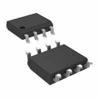
LMC6032IMX/NOPB National Semiconductor, LMC6032IMX/NOPB Datasheet - Page 8

LMC6032IMX/NOPB
Manufacturer Part Number
LMC6032IMX/NOPB
Description
IC OP AMP DUAL CMOS 8-SOIC
Manufacturer
National Semiconductor
Datasheet
1.LMC6032IMNOPB.pdf
(14 pages)
Specifications of LMC6032IMX/NOPB
Amplifier Type
General Purpose
Number Of Circuits
2
Slew Rate
1.1 V/µs
Gain Bandwidth Product
1.4MHz
Current - Input Bias
0.04pA
Voltage - Input Offset
1000µV
Current - Supply
750µA
Current - Output / Channel
40mA
Voltage - Supply, Single/dual (±)
4.75 V ~ 15.5 V, ±2.38 V ~ 7.75 V
Operating Temperature
-40°C ~ 85°C
Mounting Type
Surface Mount
Package / Case
8-SOIC (3.9mm Width)
Number Of Channels
2
Voltage Gain Db
126.02 dB
Common Mode Rejection Ratio (min)
60 dB
Input Voltage Range (max)
15.5 V
Input Voltage Range (min)
4.75 V
Input Offset Voltage
9 mV
Operating Supply Voltage
5 V, 9 V, 12 V, 15 V
Supply Current
0.38 mA
Maximum Operating Temperature
+ 85 C
Mounting Style
SMD/SMT
Maximum Dual Supply Voltage
+/- 7.75 V
Minimum Operating Temperature
- 40 C
Lead Free Status / RoHS Status
Lead free / RoHS Compliant
Output Type
-
-3db Bandwidth
-
Lead Free Status / Rohs Status
Details
Other names
*LMC6032IMX/NOPB
Available stocks
Company
Part Number
Manufacturer
Quantity
Price
Company:
Part Number:
LMC6032IMX/NOPB
Manufacturer:
TI
Quantity:
12 000
Part Number:
LMC6032IMX/NOPB
Manufacturer:
NS/国半
Quantity:
20 000
www.national.com
Application Hints
where
is the amplifier’s low-frequency noise gain and GBW is the
amplifier’s gain bandwidth product. An amplifier’s low-
frequency noise gain is represented by the formula
regardless of whether the amplifier is being used in an
inverting or non-inverting mode. Note that a feedback ca-
pacitor is more likely to be needed when the noise gain is low
and/or the feedback resistor is large.
If the above condition is met (indicating a feedback capacitor
will probably be needed), and the noise gain is large enough
that:
the following value of feedback capacitor is recommended:
If
the feedback capacitor should be:
Note that these capacitor values are usually significantly
smaller than those given by the older, more conservative
formula:
(Continued)
8
C
from the circuit board and socket. C
C
Using the smaller capacitors will give much higher band-
width with little degradation of transient response. It may be
necessary in any of the above cases to use a somewhat
larger feedback capacitor to allow for unexpected stray ca-
pacitance, or to tolerate additional phase shifts in the loop, or
excessive capacitive load, or to decrease the noise or band-
width, or simply because the particular circuit implementa-
tion needs more feedback capacitance to be sufficiently
stable. For example, a printed circuit board’s stray capaci-
tance may be larger or smaller than the breadboard’s, so the
actual optimum value for C
estimated using the breadboard. In most cases, the value of
C
computed value.
CAPACITIVE LOAD TOLERANCE
Like many other op amps, the LMC6032 may oscillate when
its applied load appears capacitive. The threshold of oscilla-
tion varies both with load and circuit gain. The configuration
most sensitive to oscillation is a unity-gain follower. See the
Typical Performance Characteristics.
The load capacitance interacts with the op amp’s output
resistance to create an additional pole. If this pole frequency
is sufficiently low, it will degrade the op amp’s phase margin
so that the amplifier is no longer stable at low gains. As
shown in Figure 3, the addition of a small resistor (50Ω to
100Ω) in series with the op amp’s output, and a capacitor (5
pF to 10 pF) from inverting input to output pins, returns the
phase margin to a safe value without interfering with lower-
frequency circuit operation. Thus, larger values of capaci-
tance can be tolerated without oscillation. Note that in all
cases, the output will ring heavily when the load capacitance
is near the threshold for oscillation.
Capacitive load driving capability is enhanced by using a pull
up resistor to V
conducting 500 µA or more will significantly improve capaci-
FIGURE 3. Rx, Cx Improve Capacitive Load Tolerance
S
S
F
consists of the amplifier’s input capacitance plus any stray capacitance
and the feedback resistor.
should be checked on the actual circuit, starting with the
FIGURE 2. General Operational Amplifier Circuit
+
(Figure 4). Typically a pull up resistor
F
F
may be different from the one
compensates for the pole caused by
01113504
01113505


