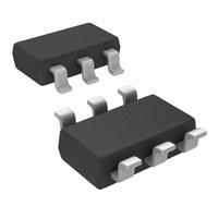
LMH6611MK/NOPB National Semiconductor, LMH6611MK/NOPB Datasheet - Page 22

LMH6611MK/NOPB
Manufacturer Part Number
LMH6611MK/NOPB
Description
IC AMP 345MHZ 3.2MA R-R TSOT23-6
Manufacturer
National Semiconductor
Series
PowerWise®r
Datasheet
1.551600074-001.pdf
(30 pages)
Specifications of LMH6611MK/NOPB
Amplifier Type
General Purpose
Number Of Circuits
1
Output Type
Rail-to-Rail
Slew Rate
460 V/µs
Gain Bandwidth Product
135MHz
-3db Bandwidth
365MHz
Current - Input Bias
6.5µA
Voltage - Input Offset
74µV
Current - Supply
3.3mA
Current - Output / Channel
120mA
Voltage - Supply, Single/dual (±)
2.7 V ~ 11 V, ±1.35 V ~ 5.5 V
Operating Temperature
-40°C ~ 125°C
Mounting Type
Surface Mount
Package / Case
TSOT-23-6, TSOT-6
For Use With
551600083-001 - BOARD FOR SOT23 LMH6611/18
Lead Free Status / RoHS Status
Lead free / RoHS Compliant
Other names
LMH6611MK
Available stocks
Company
Part Number
Manufacturer
Quantity
Price
Company:
Part Number:
LMH6611MK/NOPB
Manufacturer:
TI
Quantity:
3 400
www.national.com
Because SINAD compares all undesired frequency compo-
nents with the input frequency, it is an overall measure of an
ADC’s dynamic performance. The following sections will dis-
cuss the three different ADC driver architectures in detail.
SINGLE TO SINGLE ADC DRIVER
This architecture has a single-ended input source connected
to the input of the op amp and the single-ended output of the
op amp is then fed to the single-ended input of the ADC. The
low noise of only 10 nV/
make the LMH6611 an excellent choice for driving the 12-bit
ADC121S101 500 KSPS to 1 MSPS ADC, which has a suc-
cessive approximation architecture with internal sample and
hold circuits.
in a 2nd order multiple-feedback with gain of −1 (inverting)
configuration, driving an ADC121S101. The inverting config-
When the op amp and the ADC are using the same supply, it
is important that both devices are well bypassed. A 0.1 µF
ceramic capacitor and a 10 µF tantalum capacitor should be
located as close as possible to each supply pin. A sample
layout is shown in
C6) and the 10 µF capacitors (C11 and C5) are located very
close to the supply pins of the LMH6611 and the AD-
C121S101.
The following are recommendations for the design of PCB
layout in order to obtain the optimum high frequency perfor-
mance:
Output/ADC Input
Amplifier
4
Figure 2
Figure
shows the schematic of the LMH6611
TABLE 1. Performance of the LMH6611 Combined with the ADC121S101
5. The 0.1 µF capacitors (C13 and
and a wide bandwidth of 345 MHz
SINAD
(dB)
70.2
FIGURE 4. Single to Single ADC Driver
SNR
(dB)
71.6
−75.7
THD
(dB)
22
uration is preferred over the non-inverting configuration, as it
offers more linear output response.
formance data of the LMH6611 combined with the AD-
C121S101. The ADC driver’s cutoff frequency of 500 kHz is
found from the equation:
The op amp’s gain is set by the equation:
•
•
•
•
•
SFDR
(dBc)
77.6
Place ADC and amplifier as close together as possible.
Put the supply bypassing capacitors as close as possible
to the device (<1”).
Utilize surface mount instead of through-hole components
and ground and power planes.
Keep the traces short where possible.
Use terminated transmission lines for long traces.
ENOB
11.4
ADC121S101 @ f = 200 kHz
Table 1
Notes
shows the per-
30033629


