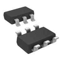
LMH6611MK/NOPB National Semiconductor, LMH6611MK/NOPB Datasheet - Page 26

LMH6611MK/NOPB
Manufacturer Part Number
LMH6611MK/NOPB
Description
IC AMP 345MHZ 3.2MA R-R TSOT23-6
Manufacturer
National Semiconductor
Series
PowerWise®r
Datasheet
1.551600074-001.pdf
(30 pages)
Specifications of LMH6611MK/NOPB
Amplifier Type
General Purpose
Number Of Circuits
1
Output Type
Rail-to-Rail
Slew Rate
460 V/µs
Gain Bandwidth Product
135MHz
-3db Bandwidth
365MHz
Current - Input Bias
6.5µA
Voltage - Input Offset
74µV
Current - Supply
3.3mA
Current - Output / Channel
120mA
Voltage - Supply, Single/dual (±)
2.7 V ~ 11 V, ±1.35 V ~ 5.5 V
Operating Temperature
-40°C ~ 125°C
Mounting Type
Surface Mount
Package / Case
TSOT-23-6, TSOT-6
For Use With
551600083-001 - BOARD FOR SOT23 LMH6611/18
Lead Free Status / RoHS Status
Lead free / RoHS Compliant
Other names
LMH6611MK
Available stocks
Company
Part Number
Manufacturer
Quantity
Price
Company:
Part Number:
LMH6611MK/NOPB
Manufacturer:
TI
Quantity:
3 400
www.national.com
DC LEVEL SHIFTING
Often a signal must be both amplified and level shifted while
using a single supply for the op amp. The circuit in
can do both of these tasks. The procedure for specifying the
resistor values is as follows.
1.
2.
3.
4.
5.
6.
7.
8.
9.
10. Calculate R
11. Calculate R
12. Calculate R
Check that both the V
ranges of the LMH6611.
4
Figure 10
tiple feedback low pass filter. This filter is set up to have a gain
th
ORDER MULTIPLE FEEDBACK LOW-PASS FILTER
Determine the input voltage.
Calculate the input voltage midpoint, V
(V
Determine the output voltage needed.
Calculate the output voltage midpoint, V
V
Calculate the gain needed, gain = (V
(V
Calculate the amount the voltage needs to be shifted
from input to output, ΔV
Set the supply voltage to be used.
Calculate the noise gain, noise gain = gain + ΔV
Set R
OUTMIN
INMAX
INMAX
shows the LMH6612 used as the amplifier in a mul-
F
.
– V
– V
+ (V
INMIN
INMIN
1
2
G
, R
, R
OUTMAX
, R
1
2
G
)/2.
)
= R
= R
= R
IN
– V
F
F
F
/gain.
/(noise gain-gain).
/(noise gain – 1).
and V
OUTMIN
OUT
= V
OUT
FIGURE 10. 4
)/2.
OUTMID
are within the voltage
OUTMAX
– gain x V
INMID
OUTMID
th
= V
– V
Order Multiple Feedback Low-Pass Filter
=
Figure 9
INMIN
OUTMIN
OUT
INMID
/V
+
.
S
)/
.
26
The following example is for a V
2V to 4V.
1.
2.
3.
4.
5.
6.
7.
8.
9.
10. R
11. R
12. R
of +1 and a −3 dB point of 1 MHz. Values can be determined
by using the WEBENCH
www.amplifiers.national.com.
V
V
V
V
Gain = (4V – 2V)/(1V – 0V) = 2
ΔV
For the example the supply voltage will be +5V.
Noise gain = 2 + 2/5V = 2.4
R
IN
INMID
OUT
OUTMID
F
1
2
G
OUT
= 2 kΩ/2 = 1 kΩ
= 2 kΩ/(2.4-2) = 5 kΩ
= 2 kΩ
= 2 kΩ/(2.4 – 1) = 1.43 kΩ
= 0V to 1V
= 2V to 4V
= 0V + (1V – 0V)/2 = 0.5V
= 3V – 2 x 0.5V = 2
= 2V + (4V – 2V)/2 = 3V
FIGURE 9. DC Level Shifting
®
Active Filter Designer found at
IN
of 0V to 1V with a V
30033648
30033628
OUT
of


