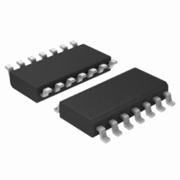
MC33074ADR2G ON Semiconductor, MC33074ADR2G Datasheet - Page 2

MC33074ADR2G
Manufacturer Part Number
MC33074ADR2G
Description
IC OPAMP QUAD 4.5MHZ 14SOIC
Manufacturer
ON Semiconductor
Type
General Purpose Amplifierr
Datasheet
1.MC33072DR2G.pdf
(25 pages)
Specifications of MC33074ADR2G
Amplifier Type
General Purpose
Number Of Circuits
4
Slew Rate
13 V/µs
Gain Bandwidth Product
4.5MHz
Current - Input Bias
100nA
Voltage - Input Offset
500µV
Current - Supply
1.9mA
Current - Output / Channel
30mA
Voltage - Supply, Single/dual (±)
3 V ~ 44 V, ±1.5 V ~ 22 V
Operating Temperature
-40°C ~ 85°C
Mounting Type
Surface Mount
Package / Case
14-SOIC (3.9mm Width), 14-SOL
Rail/rail I/o Type
No
Number Of Elements
4
Unity Gain Bandwidth Product
4.5MHz
Common Mode Rejection Ratio
80dB
Input Offset Voltage
3@5VmV
Input Bias Current
500nA
Single Supply Voltage (typ)
5/9/12/15/18/24/28V
Voltage Gain In Db
100dB
Power Supply Rejection Ratio
80dB
Power Supply Requirement
Single/Dual
Shut Down Feature
No
Single Supply Voltage (min)
3V
Single Supply Voltage (max)
44V
Dual Supply Voltage (min)
±1.5V
Dual Supply Voltage (max)
±22V
Technology
Bipolar
Operating Temp Range
-40C to 85C
Operating Temperature Classification
Industrial
Mounting
Surface Mount
Pin Count
14
Package Type
SOIC
Number Of Channels
4
Voltage Gain Db
100 dB
Common Mode Rejection Ratio (min)
80 dB
Input Voltage Range (max)
Positive Rail - 1.8 V
Input Voltage Range (min)
Negative Rail
Operating Supply Voltage
44 V
Supply Current
7.6 mA
Maximum Operating Temperature
+ 85 C
Mounting Style
SMD/SMT
Maximum Dual Supply Voltage
+/- 22 V
Minimum Operating Temperature
- 40 C
Lead Free Status / RoHS Status
Lead free / RoHS Compliant
Output Type
-
-3db Bandwidth
-
Lead Free Status / Rohs Status
Compliant
Other names
MC33074ADR2GOS
MC33074ADR2GOS
MC33074ADR2GOSTR
MC33074ADR2GOS
MC33074ADR2GOSTR
Available stocks
Company
Part Number
Manufacturer
Quantity
Price
Part Number:
MC33074ADR2G
Manufacturer:
ON/安森美
Quantity:
20 000
Stresses exceeding Maximum Ratings may damage the device. Maximum Ratings are stress ratings only. Functional operation above the
Recommended Operating Conditions is not implied. Extended exposure to stresses above the Recommended Operating Conditions may affect
device reliability.
1. Either or both input voltages should not exceed the magnitude of V
2. Power dissipation must be considered to ensure maximum junction temperature (T
MAXIMUM RATINGS
Supply Voltage (from V
Input Differential Voltage Range
Input Voltage Range
Output Short Circuit Duration (Note 2)
Operating Junction Temperature
Storage Temperature Range
Offset Null
Inputs
Inputs 1
Output 1
Inputs
CASE 626/CASE 751
V
V
EE
EE
-
+
1
2
3
4
(Single, Top View)
(Dual, Top View)
2
3
4
1
+
-
-
+
Q1
Bias
EE
-
+
Q2
8
7
6
5
to V
8
7
6
5
Output 2
V
NC
V
Output
Offset Null
CC
CC
Inputs 2
CC
Rating
Q3
Q8
)
Cancellation
Current
Base
(MC33071, MC34071 only)
Figure 1. Representative Schematic Diagram
Offset Null
R1
Inputs 1
Inputs 2
Output 1
Q4
Output 2
Q9
CASE 646/CASE 751A/CASE 948G
V
R3
Q12
D1
CC
C1
1
2
3
4
5
6
7
PIN CONNECTIONS
Q10
http://onsemi.com
(Quad, Top View)
+
-
-
+
Q13
(Each Amplifier)
R2
R4
2
1
3
4
2
CC
Q5
-
+
+
-
or V
14
13
12
11
10
9
8
Q11
Output 4
V
Output 3
EE
EE
Q14
Symbol
Inputs 4
Inputs 3
.
V
T
V
t
V
T
SC
IDR
stg
IR
S
J
Q6
J
) is not exceeded (see Figure 2).
C2
Q15
Output 1
Q7
R5
In + 1
In 1
D2
NC
Q16
Q17
−60 to +150
Indefinite
D3
(Note 1)
(Note 1)
2
3
4
R6
Value
1
+150
+44
CASE 510AJ
R7
(Top View)
VEE/GND
Current
VCC
10
Q18
Q19
5
Limit
R8
V
EE
V
/GND
CC
Output
9
8
7
6
Unit
Sec
°C
°C
V
V
V
Output 2
NC
In 2
In + 2


