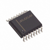
MAX691ACWE+ Maxim Integrated Products, MAX691ACWE+ Datasheet - Page 13

MAX691ACWE+
Manufacturer Part Number
MAX691ACWE+
Description
IC MPU SUPERVISOR CIRCUIT 16SOIC
Manufacturer
Maxim Integrated Products
Type
Battery Backup Circuitr
Datasheet
1.MAX691ACPE.pdf
(17 pages)
Specifications of MAX691ACWE+
Number Of Voltages Monitored
1
Output
Push-Pull, Push-Pull
Reset
Active High/Active Low
Reset Timeout
140 ms Minimum
Voltage - Threshold
4.65V
Operating Temperature
0°C ~ 70°C
Mounting Type
Surface Mount
Package / Case
16-SOIC (0.300", 7.5mm Width)
Monitored Voltage
0 V to 5.5 V
Undervoltage Threshold
4.5 V
Overvoltage Threshold
4.75 V
Manual Reset
No
Watchdog
Yes
Battery Backup Switching
Yes
Power-up Reset Delay (typ)
280 ms
Supply Voltage (max)
5.5 V
Supply Voltage (min)
0 V
Supply Current (typ)
100 uA
Maximum Power Dissipation
762 mW
Mounting Style
SMD/SMT
Maximum Operating Temperature
+ 70 C
Chip Enable Signals
Yes
Minimum Operating Temperature
0 C
Output Type
Active High or Active Low or Open Drain
Power Fail Detection
Yes
Lead Free Status / RoHS Status
Lead free / RoHS Compliant
Figure 10. Alternate CE Gating
If using separate power supplies for V
VBATT must be less than 0.3V above V
above the reset threshold. As described in the previ-
ous section, if VBATT exceeds this limit and power is
lost at V
V
switch until the circuit is broken (Figure 8).
Using memory devices with both CE and CE inputs
allows the CE loop to be bypassed. To do this, con-
nect CE IN to ground, pull up CE OUT to V
connect
device (Figure 10). The CE input of each part then
connects directly to the chip-select logic, which does
not have to be gated.
Hysteresis adds a noise margin to the power-fail com-
parator and prevents repeated triggering of PFO when
V
11 shows how to add hysteresis to the power-fail com-
IN
CC
*MAXIMUM Rp VALUE DEPENDS ON
is near the power-fail comparator trip point. Figure
THE NUMBER OF RAMS.
MINIMUM Rp VALUE IS 1kΩ.
via the VBATT-to-V
CC
–
CE OUT to the CE input of each memory
, current flows continuously from VBATT to
CE IN
Using Separate Power Supplies
MAX800M
MAX691A
MAX693A
MAX800L
V
GND
OUT
Alternate Chip-Enable Gating
______________________________________________________________________________________
CE OUT
Adding Hysteresis to the
Rp*
OUT
Power-Fail Comparator
Microprocessor Supervisory Circuits
diode and the V
for VBATT and V
ACTIVE-HIGH
FROM LOGIC
CE LINES
CC
CC
CE
CE
CE
CE
CE
CE
CE
CE
when V
and VBATT,
OUT
OUT
-to-V
RAM 1
RAM 2
RAM 3
RAM 4
, and
CC
CC
CC
is
Figure 11. Adding Hysteresis to the Power-Fail Comparator
Figure 12. Monitoring a Negative Voltage
PFO
NOTE: V
5 - 1.25 = 1.25 - V
5V
0V
R1
+5V
PFO
R2
R1
5V
0V
V
V
TRIP
TRIP
H
V
0V
= 1.25/
IN
IS NEGATIVE.
= 1.25
R2
R2
R1
TRIP
R1 + R2 I I R3
V-
TO μP
R1 + R2
R2 I I R3
R2
C1*
R3
V
V-
TRIP
PFI
PFI
PFO
V
MAX800M
MAX800M
L
V
MAX691A
MAX693A
MAX800L
MAX691A
MAX693A
MAX800L
L
- 1.25
R1
GND
GND
V
+5V
V
V
CC
CC
TRIP
V
IN
+
5 - 1.25
V
R3
H
PFO
0V
*OPTIONAL
=
1.25
R2
13


