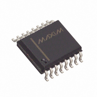
MAX691ACWE+ Maxim Integrated Products, MAX691ACWE+ Datasheet - Page 4

MAX691ACWE+
Manufacturer Part Number
MAX691ACWE+
Description
IC MPU SUPERVISOR CIRCUIT 16SOIC
Manufacturer
Maxim Integrated Products
Type
Battery Backup Circuitr
Datasheet
1.MAX691ACPE.pdf
(17 pages)
Specifications of MAX691ACWE+
Number Of Voltages Monitored
1
Output
Push-Pull, Push-Pull
Reset
Active High/Active Low
Reset Timeout
140 ms Minimum
Voltage - Threshold
4.65V
Operating Temperature
0°C ~ 70°C
Mounting Type
Surface Mount
Package / Case
16-SOIC (0.300", 7.5mm Width)
Monitored Voltage
0 V to 5.5 V
Undervoltage Threshold
4.5 V
Overvoltage Threshold
4.75 V
Manual Reset
No
Watchdog
Yes
Battery Backup Switching
Yes
Power-up Reset Delay (typ)
280 ms
Supply Voltage (max)
5.5 V
Supply Voltage (min)
0 V
Supply Current (typ)
100 uA
Maximum Power Dissipation
762 mW
Mounting Style
SMD/SMT
Maximum Operating Temperature
+ 70 C
Chip Enable Signals
Yes
Minimum Operating Temperature
0 C
Output Type
Active High or Active Low or Open Drain
Power Fail Detection
Yes
Lead Free Status / RoHS Status
Lead free / RoHS Compliant
Microprocessor Supervisory Circuits
ELECTRICAL CHARACTERISTICS (continued)
(MAX691A, MAX800L: V
unless otherwise noted.)
4
Note 1: Either V
Note 2: The supply current drawn by the MAX691A/MAX800L/MAX800M from the battery excluding I
Note 3: “+” = battery-discharging current, “--” = battery-charging current.
Note 4: Although presented as typical values, the number of clock cycles for the reset and watchdog timeout periods are fixed and
Note 5: RESET is an open-drain output and sinks current only.
Note 6: WDI is internally connected to a voltage divider between V
Note 7: The chip-enable resistance is tested with V
Note 8: The chip-enable propagation delay is measured from the 50% point at CE IN to the 50% point at CE OUT.
POWER-FAIL COMPARATOR
CHIP-ENABLE GATING
INTERNAL OSCILLATOR
PFI Input Threshold
PFI Leakage Current
PFO Output Voltage
PFO Output Short-Circuit
Current
PFI-to-PFO Delay
CE IN Leakage Current
CE IN-to-CE OUT Resistance
(Note 7)
CE OUT Short-Circuit Current
(Reset Active)
CE IN-to-CE OUT Propagation
Delay (Note 8)
CE OUT Output-Voltage High
(Reset Active)
RESET-to-CE OUT Delay
OSC IN Leakage Current
OSC IN Input Pullup Current
OSC SEL Input Pullup Current
OSC IN Frequency Range
OSC IN External Oscillator
Threshold Voltage
OSC IN Frequency with
External Capacitor
_______________________________________________________________________________________
PARAMETER
when (VBATT - 1V) < V
do not vary with process or temperature.
disabling the watchdog function.
MAX693A/MAX800M. CE IN = CE OUT = V
CC
or VBATT can go to 0V, if the other is greater than 2.0V.
CC
= +4.75V to +5.5V; MAX693A, MAX800M: V
CC
MAX69_AC/AE/AM, V
MAX800_C/E, V
I
I
Output source current
V
V
Disable mode
Enable mode
Disable mode,
50Ω source impedance driver, C
V
V
Power-down
OSC SEL = 0V
OSC SEL = V
OSC SEL = 0V
OSC SEL = 0V
V
V
OSC SEL = 0V, COSC = 47pF
SINK
SOURCE
< VBATT. In most applications, this is a brief period as V
IN
IN
CC
CC
IH
IL
= -20mV, V
= 20mV, V
= 5V, I
= 0V, VBATT = 2.8V, I
= 3.2mA
= 1µA, V
OUT
OUT
OD
OD
–
CE OUT = 0V
CC
= -100µA
CONDITIONS
CC
CC
CC
= 15mV
or floating, OSC IN = 0V
= 15mV
= 5V
/2.
= +4.75V for the MAX691A/MAX800L and V
= 5V
CC
= 5V
OUT
= 1µA
LOAD
OUT
and GND. If unconnected, WDI is driven to 1.6V (typ),
= 50pF
CC
= +4.5V to +5.5V; VBATT = 2.8V, T
V
OUT
1.225
MIN
1.2
3.5
0.1
3.5
2.7
1
- 0.3
CC
falls through this region.
V
CC
OUT
±0.005
±0.01
TYP
1.25
1.25
0.75
0.10
3.65
100
OUT
15
25
60
75
12
10
10
50
= +4.5V for the
6
- 0.6
typically goes to 10µA
MAX
1.275
A
2.00
±25
100
150
100
100
1.3
0.4
2.0
±1
10
±5
= T
MIN
UNITS
to T
kHz
kHz
mA
nA
µA
µA
µA
µA
µA
µs
ns
µs
Ω
V
V
V
V
MAX
,


