LM3940IS-3.3/NOPB National Semiconductor, LM3940IS-3.3/NOPB Datasheet - Page 3
LM3940IS-3.3/NOPB
Manufacturer Part Number
LM3940IS-3.3/NOPB
Description
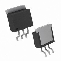
IC REGULATOR LDO 3.3V TO-263
Manufacturer
National Semiconductor
Datasheet
1.LM3940IMP-3.3NOPB.pdf
(12 pages)
Specifications of LM3940IS-3.3/NOPB
Regulator Topology
Positive Fixed
Voltage - Output
3.3V
Voltage - Input
Up to 7.5V
Voltage - Dropout (typical)
0.5V @ 1A
Number Of Regulators
1
Current - Output
1A
Operating Temperature
-40°C ~ 125°C
Mounting Type
Surface Mount
Package / Case
TO-263-3, D²Pak (3 leads + Tab), TO-263AA
Number Of Outputs
1
Polarity
Positive
Input Voltage Max
7.5 V
Output Voltage
3.3 V
Output Type
Fixed
Dropout Voltage (max)
0.8 V At 1 A
Output Current
1 A
Line Regulation
40 mV
Load Regulation
50 mV
Maximum Operating Temperature
+ 125 C
Mounting Style
SMD/SMT
Minimum Operating Temperature
- 40 C
Lead Free Status / RoHS Status
Lead free / RoHS Compliant
Current - Limit (min)
-
Lead Free Status / Rohs Status
Details
Other names
*LM3940IS-3.3
*LM3940IS-3.3/NOPB
LM3940IS-3.3
*LM3940IS-3.3/NOPB
LM3940IS-3.3
Available stocks
Company
Part Number
Manufacturer
Quantity
Price

Part Number:
LM3940IS-3.3/NOPB
Manufacturer:
TI/德州仪器
Quantity:
20 000


Absolute Maximum Ratings
If Military/Aerospace specified devices are required,
please contact the National Semiconductor Sales Office/
Distributors for availability and specifications.
Electrical Characteristics
Limits in standard typeface are for T
otherwise specified: V
Thermal Performance
Note 1: Absolute maximum ratings indicate limits beyond which damage to the component may occur. Electrical specifications do not apply when operating the
device outside of its rated operating conditions.
Note 2: The maximum allowable power dissipation is a function of the maximum junction temperature, T
the ambient temperature, T
shutdown. The value of θ
SOT-223 package. The effective value of θ
θ
and power dissipation for the LLP package, refer to Application Note AN-1187. The θ
under the exposed pad.
Note 3: ESD rating is based on the human body model: 100 pF discharged through 1.5 kΩ.
Note 4: All limits guaranteed for T
via correlation using standard Statistical Quality Control (SQC) methods.
Note 5: Dropout voltage is defined as the input-output differential voltage where the regulator output drops to a value that is 100 mV below the value that is
measured at V
Storage Temperature Range
Lead Temperature (Soldering, 5 seconds)
Power Dissipation (Note 2)
JA
Symbol
Junction-to-Ambient, θ
I
for the LLP package is specifically dependant on PCB trace area, trace material, and the number of layers and thermal vias. For improved thermal resistance
L
Junction-to-Case, θ
V
(SC)
V
Z
Thermal Resistance
Thermal Resistance
I
e
DO
Q
O
O
n
IN
= 5V.
Output Voltage
Line Regulation
Load Regulation
Output Impedance
Quiescent Current
Output Noise Voltage
Dropout Voltage
(Note 5)
Short Circuit Current
JA
IN
A
(for devices in still air with no heatsink) is 60°C/W for the TO-220 package, 80°C/W for the TO-263 package, and 174°C/W for the
. Exceeding the maximum allowable power dissipation will cause excessive die temperature, and the regulator will go into thermal
JC
= 5V, I
Parameter
JA
J
= 25°C are 100% tested and are used to calculate Outgoing Quality Levels. All limits at temperature extremes are guaranteed
L
= 1A, C
3-Lead TO-220
3-Lead TO-263
8-Lead LLP
3-Lead TO-220
3-Lead TO-263
8-Lead LLP (Note 2)
JA
J
can be reduced by using a heatsink (see Application Hints for specific information on heatsinking). The value of
= 25°C, and limits in boldface type apply over the full operating temperature range. Unless
OUT
−65°C to +150°C
Internally Limited
= 33 μF.
5 mA
I
4.5V
50 mA
I
I
f = 120 Hz
4.5V
I
V
I
BW = 10 Hz–100 kHz
I
I
I
R
L
L
L
L
L
L
L
L
(Note 1)
IN
L
= 5 mA
(DC) = 100 mA
(AC) = 20 mA (rms)
= 5 mA
= 1A
= 5 mA
= 1A
= 100 mA
= 0
= 5V
≤
≤
≤
260°C
≤
V
V
I
L
IN
IN
Conditions
I
L
≤
≤
≤
≤
1A
5.5V
5.5V
1A
3
Operating Ratings
JA
Input Supply Voltage
ESD Rating (Note 3)
Junction Temperature Range, T
Input Supply Voltage, V
rating for the LLP is with a JESD51-7 test board having 6 thermal vias
Typical
110
150
110
3.3
0.5
1.7
20
35
35
10
J
, the junction-to-ambient thermal resistance, θ
60
80
35
4
4
6
IN(MIN)
LM3940 (Note 4)
3.20
3.13
min
1.2
J
(Note 1)
max
3.40
3.47
200
250
150
200
0.8
1.0
40
50
80
15
20
−40°C to +125°C
www.national.com
V
μV (rms)
O
Units
°C/W
°C/W
°C/W
°C/W
°C/W
°C/W
mV
mΩ
mA
mV
+ V
JA
V
V
A
7.5V
2 kV
, and
DO
Related parts for LM3940IS-3.3/NOPB
Image
Part Number
Description
Manufacturer
Datasheet
Request
R

Part Number:
Description:
V REG LDO +3.3V, 3940, SOT-263-3
Manufacturer:
National Semiconductor
Datasheet:

Part Number:
Description:
National Semiconductor [8-Bit D/A Converter]
Manufacturer:
National Semiconductor
Datasheet:
Part Number:
Description:
National Semiconductor [Media Coprocessor]
Manufacturer:
National Semiconductor
Datasheet:
Part Number:
Description:
Digitally Controlled Tone and Volume Circuit with Stereo Audio Power Amplifier, Microphone Preamp Stage and National 3D Sound
Manufacturer:
National Semiconductor
Datasheet:
Part Number:
Description:
Digitally Controlled Tone and Volume Circuit with Stereo Audio Power Amplifier, Microphone Preamp Stage and National 3D Sound
Manufacturer:
National Semiconductor
Datasheet:
Part Number:
Description:
AC97 Rev 2 Codec with Sample Rate Conversion and National 3D Sound
Manufacturer:
National Semiconductor
Part Number:
Description:
Manufacturer:
National Semiconductor
Datasheet:
Part Number:
Description:
Manufacturer:
National Semiconductor
Datasheet:
Part Number:
Description:
General Purpose, Low Voltage, Low Power, Rail-to-Rail Output Operational Amplifiers
Manufacturer:
National Semiconductor
Datasheet:
Part Number:
Description:
8-bit 20 MSPS flash A/D converter.
Manufacturer:
National Semiconductor
Datasheet:
Part Number:
Description:
Low Noise Quad Operational Amplifier
Manufacturer:
National Semiconductor
Datasheet:
Part Number:
Description:
Quad Differential Line Receivers
Manufacturer:
National Semiconductor
Datasheet:
Part Number:
Description:
Quad High Speed Trapezoidal? Bus Transceiver
Manufacturer:
National Semiconductor
Datasheet:
Part Number:
Description:
Dual Line Receiver
Manufacturer:
National Semiconductor
Datasheet: