LM3940IS-3.3/NOPB National Semiconductor, LM3940IS-3.3/NOPB Datasheet - Page 7
LM3940IS-3.3/NOPB
Manufacturer Part Number
LM3940IS-3.3/NOPB
Description
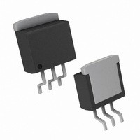
IC REGULATOR LDO 3.3V TO-263
Manufacturer
National Semiconductor
Datasheet
1.LM3940IMP-3.3NOPB.pdf
(12 pages)
Specifications of LM3940IS-3.3/NOPB
Regulator Topology
Positive Fixed
Voltage - Output
3.3V
Voltage - Input
Up to 7.5V
Voltage - Dropout (typical)
0.5V @ 1A
Number Of Regulators
1
Current - Output
1A
Operating Temperature
-40°C ~ 125°C
Mounting Type
Surface Mount
Package / Case
TO-263-3, D²Pak (3 leads + Tab), TO-263AA
Number Of Outputs
1
Polarity
Positive
Input Voltage Max
7.5 V
Output Voltage
3.3 V
Output Type
Fixed
Dropout Voltage (max)
0.8 V At 1 A
Output Current
1 A
Line Regulation
40 mV
Load Regulation
50 mV
Maximum Operating Temperature
+ 125 C
Mounting Style
SMD/SMT
Minimum Operating Temperature
- 40 C
Lead Free Status / RoHS Status
Lead free / RoHS Compliant
Current - Limit (min)
-
Lead Free Status / Rohs Status
Details
Other names
*LM3940IS-3.3
*LM3940IS-3.3/NOPB
LM3940IS-3.3
*LM3940IS-3.3/NOPB
LM3940IS-3.3
Available stocks
Company
Part Number
Manufacturer
Quantity
Price

Part Number:
LM3940IS-3.3/NOPB
Manufacturer:
TI/德州仪器
Quantity:
20 000


If a manufactured heatsink is to be selected, the value of
heatsink-to-ambient thermal resistance, θ
calculated:
θ
Where: θ
θ
When a value for θ
heatsink must be selected that has a value that is less than
or equal to this number.
θ
in the catalog, or shown in a curve that plots temperature rise
vs. power dissipation for the heatsink.
HEATSINKING TO-263 AND SOT-223 PACKAGE PARTS
Both the TO-263 (“S”) and SOT-223 (“MP”) packages use a
copper plane on the PCB and the PCB itself as a heatsink. To
optimize the heat sinking ability of the plane and PCB, solder
the tab of the package to the plane.
Figure 3 shows for the TO-263 the measured values of θ
for different copper area sizes using a typical PCB with 1
ounce copper and no solder mask over the copper area used
for heatsinking.
FIGURE 3. θ
As shown in the figure, increasing the copper area beyond 1
square inch produces very little improvement. It should also
be observed that the minimum value of θ
package mounted to a PCB is 32°C/W.
As a design aid, Figure 4 shows the maximum allowable
power dissipation compared to ambient temperature for the
TO-263 device (assuming θ
junction temperature is 125°C).
(H−A)
(H−A)
= θ
is specified numerically by the heatsink manufacturer
(C−H)
(JA)
(J−C)
(JA)
− θ
is defined as the thermal resistance from the
junction to the surface of the case. A value of
4°C/W can be assumed for θ
culation.
is defined as the thermal resistance between
the case and the surface of the heatsink. The
value of θ
about 2.5°C/W (depending on method of at-
tachment, insulator, etc.). If the exact value is
unknown, 2°C/W should be assumed for θ
−H)
(C−H)
vs. Copper (1 ounce) Area for the TO-263
.
(H−A)
− θ
is found using the equation shown, a
(J−C)
(C−H)
Package
(JA)
will vary from about 1.5°C/W to
is 35°C/W and the maximum
(JA)
(H−A)
1208007
(J−C)
for the TO-263
, must first be
for this cal-
(JA)
(C
7
Figure 5 and Figure 6 show the information for the SOT-223
package. Figure 6 assumes a θ
copper and 51°C/W for 2 ounce copper and a maximum junc-
tion temperature of 125°C.
FIGURE 5. θ
Please see AN1028 for power enhancement techniques to be
used with the SOT-223 package.
FIGURE 4. Maximum Power Dissipation vs. T
FIGURE 6. Maximum Power Dissipation vs. T
(JA)
vs. Copper (2 ounce) Area for the SOT-223
SOT-223 Package
TO-263 Package
Package
(JA)
of 74°C/W for 1 ounce
1208011
1208008
1208012
www.national.com
AMB
AMB
for the
for the
Related parts for LM3940IS-3.3/NOPB
Image
Part Number
Description
Manufacturer
Datasheet
Request
R

Part Number:
Description:
V REG LDO +3.3V, 3940, SOT-263-3
Manufacturer:
National Semiconductor
Datasheet:

Part Number:
Description:
National Semiconductor [8-Bit D/A Converter]
Manufacturer:
National Semiconductor
Datasheet:
Part Number:
Description:
National Semiconductor [Media Coprocessor]
Manufacturer:
National Semiconductor
Datasheet:
Part Number:
Description:
Digitally Controlled Tone and Volume Circuit with Stereo Audio Power Amplifier, Microphone Preamp Stage and National 3D Sound
Manufacturer:
National Semiconductor
Datasheet:
Part Number:
Description:
Digitally Controlled Tone and Volume Circuit with Stereo Audio Power Amplifier, Microphone Preamp Stage and National 3D Sound
Manufacturer:
National Semiconductor
Datasheet:
Part Number:
Description:
AC97 Rev 2 Codec with Sample Rate Conversion and National 3D Sound
Manufacturer:
National Semiconductor
Part Number:
Description:
Manufacturer:
National Semiconductor
Datasheet:
Part Number:
Description:
Manufacturer:
National Semiconductor
Datasheet:
Part Number:
Description:
General Purpose, Low Voltage, Low Power, Rail-to-Rail Output Operational Amplifiers
Manufacturer:
National Semiconductor
Datasheet:
Part Number:
Description:
8-bit 20 MSPS flash A/D converter.
Manufacturer:
National Semiconductor
Datasheet:
Part Number:
Description:
Low Noise Quad Operational Amplifier
Manufacturer:
National Semiconductor
Datasheet:
Part Number:
Description:
Quad Differential Line Receivers
Manufacturer:
National Semiconductor
Datasheet:
Part Number:
Description:
Quad High Speed Trapezoidal? Bus Transceiver
Manufacturer:
National Semiconductor
Datasheet:
Part Number:
Description:
Dual Line Receiver
Manufacturer:
National Semiconductor
Datasheet: