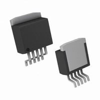
LP3891ES-1.2/NOPB National Semiconductor, LP3891ES-1.2/NOPB Datasheet

LP3891ES-1.2/NOPB
Specifications of LP3891ES-1.2/NOPB
*LP3891ES-1.2/NOPB
LP3891ES-1.2
Related parts for LP3891ES-1.2/NOPB
LP3891ES-1.2/NOPB Summary of contents
Page 1
... Typical Application Circuit At least 10 µF of input and output capacitance is required for stability. *Tantalum capacitors are recommended. Aluminum electrolytic capacitors may be used for restricted temperature range. See application hints. © 2006 National Semiconductor Corporation Features n Ultra low dropout voltage (100mV n Low ground pin current n Load regulation of 0 ...
Page 2
... Connection Diagrams TO-220, Top View Ordering Information Order Number Package Type LP3891ES-1.2 LP3891ESX-1.2 LP3891ET-1.2 LP3891ES-1.5 LP3891ESX-1.5 LP3891ET-1.5 LP3891ES-1.8 LP3891ESX-1.8 LP3891ET-1.8 LP3891EMR-1.2 LP3891EMRX-1.2 LP3891EMR-1.5 LP3891EMRX-1.5 LP3891EMR-1.8 LP3891EMRX-1.8 Block Diagram www.national.com 20069502 20069553 PSOP-8, Top View Package Drawing TO263-5 TS5B TO263-5 TS5B TO220-5 ...
Page 3
... Absolute Maximum Ratings If Military/Aerospace specified devices are required, please contact the National Semiconductor Sales Office/ Distributors for availability and specifications. Storage Temperature Range Lead Temp. (Soldering, 5 seconds) ESD Rating Human Body Model (Note 3) Machine Model (Note 10) Power Dissipation (Note 2) V Supply Voltage (Survival) ...
Page 4
Electrical Characteristics over the full operating temperature range. Unless otherwise specified µ (Continued) OUT S/D BIAS Symbol Parameter AC Parameters PSRR (V ) Ripple Rejection for V IN Voltage PSRR Ripple Rejection ...
Page 5
Typical Performance Characteristics 10µF, S/D pin is tied 2.2V, V BIAS VSD GND DC Load Regulation Line Regulation vs V Unless otherwise specified 1.8V OUT 20069505 20069507 BIAS 20069509 5 ...
Page 6
Typical Performance Characteristics 10µF, S/D pin is tied 2.2V, V BIAS VSD GND V Startup Waveform OUT Line Regulation vs V www.national.com Unless otherwise specified 1.8V (Continued) OUT 20069512 20069515 ...
Page 7
Typical Performance Characteristics 10µF, S/D pin is tied 2.2V, V BIAS IN V PSRR IN Unless otherwise specified 1.8V (Continued) OUT 20069523 7 = 25˚ µF, Cin = J OUT ...
Page 8
Application Hints EXTERNAL CAPACITORS To assure regulator stability, input and output capacitors are required as shown in the Typical Application Circuit. OUTPUT CAPACITOR At least 10µF of output capacitance is required for stability (the amount of capacitance can be increased ...
Page 9
Application Hints (Continued) HEATSINKING TO-263 PACKAGE The TO-263 package uses the copper plane on the PCB as a heatsink. The tab of these packages are soldered to the copper plane for heat sinking. The graph below shows a curve for ...
Page 10
Physical Dimensions TO220 5-lead, Molded, Stagger Bend Package (TO220-5) TO263 5-Lead, Molded, Surface Mount Package (TO263-5) www.national.com inches (millimeters) unless otherwise noted NS Package Number T05D NS Package Number TS5B 10 ...
Page 11
... BANNED SUBSTANCE COMPLIANCE National Semiconductor follows the provisions of the Product Stewardship Guide for Customers (CSP-9-111C2) and Banned Substances and Materials of Interest Specification (CSP-9-111S2) for regulatory environmental compliance. Details may be found at: www.national.com/quality/green. ...


