LP38690DT-1.8/NOPB National Semiconductor, LP38690DT-1.8/NOPB Datasheet - Page 12
LP38690DT-1.8/NOPB
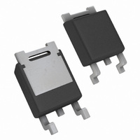
Manufacturer Part Number
LP38690DT-1.8/NOPB
Description
IC REG LDO 1A 1.8V TO-252
Manufacturer
National Semiconductor
Series
PowerWise®r
Datasheet
1.LP38690SD-3.3NOPB.pdf
(16 pages)
Specifications of LP38690DT-1.8/NOPB
Regulator Topology
Positive Fixed
Voltage - Output
1.8V
Voltage - Input
Up to 10V
Voltage - Dropout (typical)
0.95V @ 1A
Number Of Regulators
1
Current - Output
1A
Operating Temperature
-40°C ~ 125°C
Mounting Type
Surface Mount
Package / Case
TO-252-2, DPak (2 Leads + Tab), TO-252AA, SC-63
Lead Free Status / RoHS Status
Lead free / RoHS Compliant
Current - Limit (min)
-
Other names
*LP38690DT-1.8
*LP38690DT-1.8/NOPB
LP38690DT-1.8
*LP38690DT-1.8/NOPB
LP38690DT-1.8
Available stocks
Company
Part Number
Manufacturer
Quantity
Price

Part Number:
LP38690DT-1.8/NOPB
Manufacturer:
TI/德州仪器
Quantity:
20 000


www.national.com
Application Hints
EXTERNAL CAPACITORS
Like any low-dropout regulator, external capacitors are re-
quired to assure stability. These capacitors must be correctly
selected for proper performance.
INPUT CAPACITOR: An input capacitor of at least 1µF is re-
quired (ceramic recommended). The capacitor must be lo-
cated not more than one centimeter from the input pin and
returned to a clean analog ground.
OUTPUT CAPACITOR: An output capacitor is required for
loop stability. It must be located less than 1 centimeter from
the device and connected directly to the output and ground
pins using traces which have no other currents flowing
through them.
The minimum amount of output capacitance that can be used
for stable operation is 1µF. Ceramic capacitors are recom-
mended (the LP38690/2 was designed for use with ultra low
ESR capacitors). The LP38690/2 is stable with any output
capacitor ESR between zero and 100 Ohms.
ENABLE PIN (LP38692 only): The LP38692 has an enable
pin which turns the regulator output on and off. Pulling the
enable pin down to a logic low will turn the part off. The voltage
the pin has to be pulled up to in order to assure the part is on
depends on input voltage (refer to Electrical Characteristics
section). This pin should be tied to V
is not used.
Foldback Current Limiting: Foldback current limiting is built
into the LP38690/2 which reduces the amount of output cur-
rent the part can deliver as the output voltage is reduced. The
amount of load current is dependent on the differential voltage
between V
age exceeds 5V, the load current will limit at about 450 mA.
When the V
current is limited to about 1500 mA.
SELECTING A CAPACITOR
It is important to note that capacitance tolerance and variation
with temperature must be taken into consideration when se-
lecting a capacitor so that the minimum required amount of
capacitance is provided over the full operating temperature
range.
Capacitor Characteristics
CERAMIC: For values of capacitance in the 10 to 100 µF
range, ceramics are usually larger and more costly than tan-
talums but give superior AC performance for bypassing high
frequency noise because of very low ESR (typically less than
10 mΩ). However, some dielectric types do not have good
capacitance characteristics as a function of voltage and tem-
perature.
Z5U and Y5V dielectric ceramics have capacitance that drops
severely with applied voltage. A typical Z5U or Y5V capacitor
can lose 60% of its rated capacitance with half of the rated
voltage applied to it. The Z5U and Y5V also exhibit a severe
temperature effect, losing more than 50% of nominal capac-
itance at high and low limits of the temperature range.
X7R and X5R dielectric ceramic capacitors are strongly rec-
ommended if ceramics are used, as they typically maintain a
capacitance range within ±20% of nominal over full operating
ratings of temperature and voltage. Of course, they are typi-
cally larger and more costly than Z5U/Y5U types for a given
voltage and capacitance.
TANTALUM: Solid Tantalum capacitors have good temper-
ature stability: a high quality Tantalum will typically show a
IN
IN
and V
- V
OUT
OUT
differential is reduced below 4V, load
. Typically, when this differential volt-
IN
if the enable function
12
capacitance value that varies less than 10-15% across the full
temperature range of -40°C to +125°C. ESR will vary only
about 2X going from the high to low temperature limits.
PCB LAYOUT
Good PC layout practices must be used or instability can be
induced because of ground loops and voltage drops. The in-
put and output capacitors must be directly connected to the
input, output, and ground pins of the regulator using traces
which do not have other currents flowing in them (Kelvin con-
nect).
The best way to do this is to lay out C
device with short traces to the V
regulator ground pin should be connected to the external cir-
cuit ground so that the regulator and its capacitors have a
"single point ground".
It should be noted that stability problems have been seen in
applications where "vias" to an internal ground plane were
used at the ground points of the IC and the input and output
capacitors. This was caused by varying ground potentials at
these nodes resulting from current flowing through the ground
plane. Using a single point ground technique for the regulator
and it’s capacitors fixed the problem. Since high current flows
through the traces going into V
Kelvin connect the capacitor leads to these pins so there is
no voltage drop in series with the input and output capacitors.
RFI/EMI SUSCEPTIBILITY
RFI (radio frequency interference) and EMI (electromagnetic
interference) can degrade any integrated circuit’s perfor-
mance because of the small dimensions of the geometries
inside the device. In applications where circuit sources are
present which generate signals with significant high frequen-
cy energy content (> 1 MHz), care must be taken to ensure
that this does not affect the IC regulator.
If RFI/EMI noise is present on the input side of the regulator
(such as applications where the input source comes from the
output of a switching regulator), good ceramic bypass capac-
itors must be used at the input pin of the IC.
If a load is connected to the IC output which switches at high
speed (such as a clock), the high-frequency current pulses
required by the load must be supplied by the capacitors on
the IC output. Since the bandwidth of the regulator loop is less
than 100 kHz, the control circuitry cannot respond to load
changes above that frequency. This means the effective out-
put impedance of the IC at frequencies above 100 kHz is
determined only by the output capacitor(s).
In applications where the load is switching at high speed, the
output of the IC may need RF isolation from the load. It is
recommended that some inductance be placed between the
output capacitor and the load, and good RF bypass capacitors
be placed directly across the load.
PCB layout is also critical in high noise environments, since
RFI/EMI is easily radiated directly into PC traces. Noisy cir-
cuitry should be isolated from "clean" circuits where possible,
and grounded through a separate path. At MHz frequencies,
ground planes begin to look inductive and RFI/ EMI can cause
ground bounce across the ground plane. In multi-layer PCB
applications, care should be taken in layout so that noisy
power and ground planes do not radiate directly into adjacent
layers which carry analog power and ground.
OUTPUT NOISE
Noise is specified in two ways: Spot Noise or Output Noise
Density is the RMS sum of all noise sources, measured at
the regulator output, at a specific frequency (measured with
IN
, V
IN
OUT
and coming from V
, and ground pins. The
IN
and C
OUT
near the
OUT
,
Related parts for LP38690DT-1.8/NOPB
Image
Part Number
Description
Manufacturer
Datasheet
Request
R

Part Number:
Description:
IC REG LDO 1A 5.0V TO-252
Manufacturer:
National Semiconductor
Datasheet:
Part Number:
Description:
IC REG LDO 1A 3.3V TO-252
Manufacturer:
National Semiconductor
Datasheet:
Part Number:
Description:
IC REG LDO 1A 2.5V TO-252
Manufacturer:
National Semiconductor
Datasheet:

Part Number:
Description:
IC,VOLT REGULATOR,FIXED,+3.3V,CMOS,SIP,3PIN,PLASTIC
Manufacturer:
National Semiconductor
Datasheet:
Part Number:
Description:
IC,VOLT REGULATOR,FIXED,+1.8V,CMOS,SIP,3PIN,PLASTIC
Manufacturer:
National Semiconductor
Part Number:
Description:
IC,VOLT REGULATOR,FIXED,+2.5V,CMOS,SIP,3PIN,PLASTIC
Manufacturer:
National Semiconductor
Part Number:
Description:
IC,VOLT REGULATOR,FIXED,+5V,CMOS,SIP,3PIN,PLASTIC
Manufacturer:
National Semiconductor
Part Number:
Description:
National Semiconductor [8-Bit D/A Converter]
Manufacturer:
National Semiconductor
Datasheet:
Part Number:
Description:
National Semiconductor [Media Coprocessor]
Manufacturer:
National Semiconductor
Datasheet:
Part Number:
Description:
Digitally Controlled Tone and Volume Circuit with Stereo Audio Power Amplifier, Microphone Preamp Stage and National 3D Sound
Manufacturer:
National Semiconductor
Datasheet:
Part Number:
Description:
Digitally Controlled Tone and Volume Circuit with Stereo Audio Power Amplifier, Microphone Preamp Stage and National 3D Sound
Manufacturer:
National Semiconductor
Datasheet:
Part Number:
Description:
AC97 Rev 2 Codec with Sample Rate Conversion and National 3D Sound
Manufacturer:
National Semiconductor
Part Number:
Description:
Manufacturer:
National Semiconductor
Datasheet:
Part Number:
Description:
Manufacturer:
National Semiconductor
Datasheet: