LP38690DT-1.8/NOPB National Semiconductor, LP38690DT-1.8/NOPB Datasheet - Page 5
LP38690DT-1.8/NOPB
Manufacturer Part Number
LP38690DT-1.8/NOPB
Description
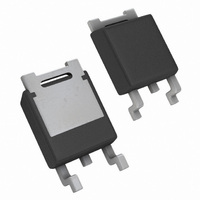
IC REG LDO 1A 1.8V TO-252
Manufacturer
National Semiconductor
Series
PowerWise®r
Datasheet
1.LP38690SD-3.3NOPB.pdf
(16 pages)
Specifications of LP38690DT-1.8/NOPB
Regulator Topology
Positive Fixed
Voltage - Output
1.8V
Voltage - Input
Up to 10V
Voltage - Dropout (typical)
0.95V @ 1A
Number Of Regulators
1
Current - Output
1A
Operating Temperature
-40°C ~ 125°C
Mounting Type
Surface Mount
Package / Case
TO-252-2, DPak (2 Leads + Tab), TO-252AA, SC-63
Lead Free Status / RoHS Status
Lead free / RoHS Compliant
Current - Limit (min)
-
Other names
*LP38690DT-1.8
*LP38690DT-1.8/NOPB
LP38690DT-1.8
*LP38690DT-1.8/NOPB
LP38690DT-1.8
Available stocks
Company
Part Number
Manufacturer
Quantity
Price

Part Number:
LP38690DT-1.8/NOPB
Manufacturer:
TI/德州仪器
Quantity:
20 000


e
V
V
I
EN
n
O
EN
Note 1: Absolute maximum ratings indicate limits beyond which damage to the component may occur. Operating ratings indicate conditions for which the device
is intended to be functional, but do not guarantee specific performance limits. For guaranteed specifications, see Electrical Characteristics. Specifications do not
apply when operating the device outside of its rated operating conditions.
Note 2: At elevated temperatures, device power dissipation must be derated based on package thermal resistance and heatsink values (if a heatsink is used).
The junction-to-ambient thermal resistance ( θ
copper area (less than 0.1 square inch). If one square inch of copper is used as a heat dissipator for the TO-252, the θ
SOT-223 package has a θ
when soldered to a copper area of one square inch. The θ
of thermal vias used (refer to application note AN-1187). If power disspation causes the junction temperature to exceed specified limits, the device will go into
thermal shutdown.
Note 3: ESD is tested using the human body model which is a 100pF capacitor discharged through a 1.5k resistor into each pin.
Note 4: Typical numbers represent the most likely parametric norm for 25°C operation.
Note 5: If used in a dual-supply system where the regulator load is returned to a negative supply, the output pin must be diode clamped to ground.
Note 6: Output voltage line regulation is defined as the change in output voltage from nominal value resulting from a change in input voltage.
Note 7: Output voltage load regulation is defined as the change in output voltage from nominal value as the load current increases from 1mA to full load.
Note 8: Dropout voltage is defined as the minimum input to output differential required to maintain the output within 100mV of nominal value.
Symbol
(LEAK)
Output Noise
Output Leakage Current
Enable Voltage (LP38692 Only)
Enable Pin Leakage
J-A
of approximately 125°C/W when soldered down to a minimum sized pattern (less than 0.1 square inch) and approximately 70°C/W
Parameter
J-A
) for the TO-252 is approximately 90°C/W for a PC board mounting with the device soldered down to minimum
J-A
BW = 10Hz to 10kHz
V
V
Output = OFF
Output = ON, V
Output = ON, V
Output = ON, V
V
values for the LLP package are also dependent on trace area, copper thickness, and the number
O
O
EN
= 3.3V
= V
= 0V or 10V, V
O
(NOM) + 1V @ 10V
Conditions
5
IN
IN
IN
= 4V
= 6V
= 10V
IN
= 10V
IN
MIN
1.8
3.0
4.0
-1
J-A
TYP (Note
drops to approximately 50°C/W. The
0.001
0.7
0.5
4)
MAX
0.4
12
1
www.national.com
µV/
Units
µA
µA
V
Related parts for LP38690DT-1.8/NOPB
Image
Part Number
Description
Manufacturer
Datasheet
Request
R

Part Number:
Description:
IC REG LDO 1A 5.0V TO-252
Manufacturer:
National Semiconductor
Datasheet:
Part Number:
Description:
IC REG LDO 1A 3.3V TO-252
Manufacturer:
National Semiconductor
Datasheet:
Part Number:
Description:
IC REG LDO 1A 2.5V TO-252
Manufacturer:
National Semiconductor
Datasheet:

Part Number:
Description:
IC,VOLT REGULATOR,FIXED,+3.3V,CMOS,SIP,3PIN,PLASTIC
Manufacturer:
National Semiconductor
Datasheet:
Part Number:
Description:
IC,VOLT REGULATOR,FIXED,+1.8V,CMOS,SIP,3PIN,PLASTIC
Manufacturer:
National Semiconductor
Part Number:
Description:
IC,VOLT REGULATOR,FIXED,+2.5V,CMOS,SIP,3PIN,PLASTIC
Manufacturer:
National Semiconductor
Part Number:
Description:
IC,VOLT REGULATOR,FIXED,+5V,CMOS,SIP,3PIN,PLASTIC
Manufacturer:
National Semiconductor
Part Number:
Description:
National Semiconductor [8-Bit D/A Converter]
Manufacturer:
National Semiconductor
Datasheet:
Part Number:
Description:
National Semiconductor [Media Coprocessor]
Manufacturer:
National Semiconductor
Datasheet:
Part Number:
Description:
Digitally Controlled Tone and Volume Circuit with Stereo Audio Power Amplifier, Microphone Preamp Stage and National 3D Sound
Manufacturer:
National Semiconductor
Datasheet:
Part Number:
Description:
Digitally Controlled Tone and Volume Circuit with Stereo Audio Power Amplifier, Microphone Preamp Stage and National 3D Sound
Manufacturer:
National Semiconductor
Datasheet:
Part Number:
Description:
AC97 Rev 2 Codec with Sample Rate Conversion and National 3D Sound
Manufacturer:
National Semiconductor
Part Number:
Description:
Manufacturer:
National Semiconductor
Datasheet:
Part Number:
Description:
Manufacturer:
National Semiconductor
Datasheet: