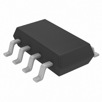
LT3060ITS8#TRMPBF Linear Technology, LT3060ITS8#TRMPBF Datasheet - Page 15

LT3060ITS8#TRMPBF
Manufacturer Part Number
LT3060ITS8#TRMPBF
Description
IC REG LDO ADJ .1A 8TSOT
Manufacturer
Linear Technology
Datasheet
1.LT3060EDCTRMPBF.pdf
(26 pages)
Specifications of LT3060ITS8#TRMPBF
Regulator Topology
Positive Adjustable
Voltage - Output
0.6 ~ 44.5 V
Voltage - Input
1.6 ~ 45 V
Voltage - Dropout (typical)
0.3V @ 100mA
Number Of Regulators
1
Current - Output
100mA
Current - Limit (min)
110mA
Operating Temperature
-40°C ~ 125°C
Mounting Type
Surface Mount
Package / Case
TSOT-23-8, TSOT-8
Lead Free Status / RoHS Status
Lead free / RoHS Compliant
Available stocks
Company
Part Number
Manufacturer
Quantity
Price
pin FuncTions
REF/BYP (Pin 1/Pin 8): Reference/Bypass. Connecting
a single capacitor from this pin to GND bypasses the
LT3060’s reference noise and soft-starts the reference.
A 10nF bypass capacitor typically reduces output voltage
noise to 30µV
start time is directly proportional to the REF/BYP capacitor
value. If the LT3060 is placed in shutdown, REF/BYP is
actively pulled low by an internal device to reset soft-start.
If low noise or soft-start performance is not required, this
pin must be left floating (unconnected). Do not drive this
pin with any active circuitry.
ADJ (Pin 2/Pin 7): Adjust. This pin is the error amplifier’s
inverting terminal. It’s typical bias current of 15nA flows out
of the pin (see curve of ADJ Pin Bias Current vs Temperature
in the Typical Performance Characteristics section). The
ADJ pin voltage is 600mV referenced to GND.
Connecting a capacitor from ADJ to OUT reduces output
noise and improves transient response for output voltages
greater than 600mV. See the Applications Information sec-
tion for calculating the value of the feedforward capacitor.
For fixed voltage versions of the LT3060, if low noise and
fast transient response is not required, this pin must be
left floating (unconnected).
OUT (Pins 3, 4/Pin 6): Output. These pin(s) supply power to
the load. Stability requirements demand a minimum 2.2µF
ceramic output capacitor to prevent oscillations. Large
load transient applications require larger output capaci-
tors to limit peak voltage transients. See the Applications
Information section for details on transient response and
reverse output characteristics. Permissible output voltage
range is 600mV to 44.5V.
RMS
in a 10Hz to 100kHz bandwidth. Soft-
(DC8/TS8)
IN (Pins 5, 6/Pin 5): Input. These pin(s) supply power to
the device. The LT3060 requires a local IN bypass capacitor
if it is located more than six inches from the main input
filter capacitor. In general, battery output impedance rises
with frequency, so adding a bypass capacitor in battery-
powered circuits is advisable.
An input bypass capacitor in the range of 1µF to 10µF
suffices. The LT3060 withstands reverse voltages on the
IN pin with respect to its GND and OUT pins. In a reversed
input situation, such as a battery plugged in backwards,
the LT3060 behaves as if a large resistor is in series with
its input. Limited reverse current flows into the LT3060
and no reverse voltage appears at the load. The device
protects itself and the load.
SHDN (Pin 7/Pin 1): Shutdown. Pulling the SHDN pin
low puts the LT3060 into a low power state and turns
the output off. Drive the SHDN pin with either logic or an
open collector/drain with a pull-up resistor. The resistor
supplies the pull-up current to the open collector/drain
logic, normally several microamperes, and the SHDN
pin current, typically less than 3µA. If unused, connect
the SHDN pin to IN. The LT3060 does not function if the
SHDN pin is not connected. The SHDN pin cannot be
driven below GND unless tied to the IN pin. If the SHDN
pin is driven below GND while IN is powered, the output
may turn on. SHDN pin logic cannot be referenced to a
negative supply voltage.
GND (Pin 8, Exposed Pad Pin 9/Pins 2, 3, 4): Ground.
For the adjustable LT3060, connect the bottom of the ex-
ternal resistor divider that sets the output voltage directly
to GND for optimum regulation. For the DFN package, tie
exposed pad Pin 9 directly to Pin 8 and the PCB ground.
This exposed pad provides enhanced thermal performance
with its connection to the PCB ground. See the Applica-
tions Information section for thermal considerations and
calculating junction temperature.
LT3060 Series
15
3060fa


