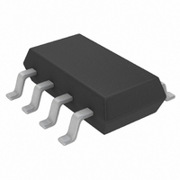
LT3060ITS8#TRMPBF Linear Technology, LT3060ITS8#TRMPBF Datasheet - Page 20

LT3060ITS8#TRMPBF
Manufacturer Part Number
LT3060ITS8#TRMPBF
Description
IC REG LDO ADJ .1A 8TSOT
Manufacturer
Linear Technology
Datasheet
1.LT3060EDCTRMPBF.pdf
(26 pages)
Specifications of LT3060ITS8#TRMPBF
Regulator Topology
Positive Adjustable
Voltage - Output
0.6 ~ 44.5 V
Voltage - Input
1.6 ~ 45 V
Voltage - Dropout (typical)
0.3V @ 100mA
Number Of Regulators
1
Current - Output
100mA
Current - Limit (min)
110mA
Operating Temperature
-40°C ~ 125°C
Mounting Type
Surface Mount
Package / Case
TSOT-23-8, TSOT-8
Lead Free Status / RoHS Status
Lead free / RoHS Compliant
Available stocks
Company
Part Number
Manufacturer
Quantity
Price
applicaTions inForMaTion
LT3060 Series
arrangement allows metal to extend beyond the ends of
the package on the topside (component side) of a PCB.
Connect this metal to GND on the PCB. The multiple IN
and OUT pins of the LT3060 also assist in spreading heat
to the PCB.
For surface mount devices, heat sinking is accomplished
by using the heat spreading capabilities of the PC board
and its copper traces. Copper board stiffeners and plated
through-holes also can spread the heat generated by
power devices.
Tables 2 and 3 list thermal resistance for several different
board sizes and copper areas. All measurements were taken
in still air on a 4 layer FR-4 board with 1oz solid internal
planes and 2oz top/bottom external trace planes with a total
board thickness of 1.6mm. The four layers were electrically
isolated with no thermal vias present. PCB layers, copper
weight, board layout and thermal vias will affect the resul-
tant thermal resistance. For more information on thermal
resistance and high thermal conductivity test boards,
refer to JEDEC standard JESD51, notably JESD51-12 and
JESD51-7. Achieving low thermal resistance necessitates
attention to detail and careful PCB layout.
Table 2. DC Package, 8-Lead DFN
*Device is mounted on topside
Table 3. TS8 Package, 8 Lead TSOT-23
*Device is mounted on topside
20
TOPSIDE*
TOPSIDE*
(mm
(mm
2500
1000
2500
1000
225
100
225
100
50
50
COPPER AREA
COPPER AREA
2
2
)
)
BACKSIDE
BACKSIDE
(mm
(mm
2500
2500
2500
2500
2500
2500
2500
2500
2500
2500
2
2
)
)
BOARD AREA
BOARD AREA
(mm
(mm
2500
2500
2500
2500
2500
2500
2500
2500
2500
2500
2
2
)
)
(JUNCTION-TO-AMBIENT)
(JUNCTION-TO-AMBIENT)
THERMAL RESISTANCE
THERMAL RESISTANCE
48°C/W
49°C/W
50°C/W
54°C/W
60°C/W
57°C/W
58°C/W
59°C/W
63°C/W
67°C/W
Calculating Junction Temperature
Example: Given an output voltage of 2.5V, an input volt-
age range of 12V ±5%, an output current range of 0mA
to 50mA and a maximum ambient temperature of 85°C,
what will the maximum junction temperature be?
The power dissipated by the device equals:
where,
So,
Using a DFN package, the thermal resistance ranges from
48°C/W to 60°C/W depending on the copper area with
no thermal vias. So the junction temperature rise above
ambient approximately equals:
The maximum junction temperature equals the maximum
ambient temperature plus the maximum junction tem-
perature rise above ambient or:
Protection Features
The LT3060 regulators incorporate several protection
features that make it ideal for use in battery-powered
circuits. In addition to the normal protection features
associated with monolithic regulators, such as current
limiting and thermal limiting, the device also protects
against reverse-input voltages, reverse-output voltages
and reverse output-to-input voltages.
Current limit protection and thermal overload protection
protect the device against current overload conditions at
the output of the device. The typical thermal shutdown
temperature is 165°C. For normal operation, do not ex-
ceed a junction temperature of 125°C (LT3060E, LT3060I,
LT3060MP) or 150°C (LT3060H).
I
I
V
I
P = 50mA • (12.6V – 2.5V) + 0.6mA • 12.6V = 0.513W
0.513W • 54°C/W = 27.8°C
T
OUT(MAX)
OUT(MAX)
GND
JMAX
IN(MAX)
at (I
= 85°C + 27.8°C = 112.8°C
= 12.6V
OUT
• (V
= 50mA
= 50mA, V
IN(MAX)
–V
OUT
IN
= 12.6V) = 0.6mA
) + I
GND
• V
IN(MAX)
3060fa


