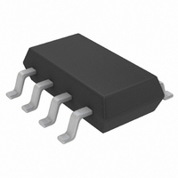
LT3060ITS8#TRMPBF Linear Technology, LT3060ITS8#TRMPBF Datasheet - Page 16

LT3060ITS8#TRMPBF
Manufacturer Part Number
LT3060ITS8#TRMPBF
Description
IC REG LDO ADJ .1A 8TSOT
Manufacturer
Linear Technology
Datasheet
1.LT3060EDCTRMPBF.pdf
(26 pages)
Specifications of LT3060ITS8#TRMPBF
Regulator Topology
Positive Adjustable
Voltage - Output
0.6 ~ 44.5 V
Voltage - Input
1.6 ~ 45 V
Voltage - Dropout (typical)
0.3V @ 100mA
Number Of Regulators
1
Current - Output
100mA
Current - Limit (min)
110mA
Operating Temperature
-40°C ~ 125°C
Mounting Type
Surface Mount
Package / Case
TSOT-23-8, TSOT-8
Lead Free Status / RoHS Status
Lead free / RoHS Compliant
Available stocks
Company
Part Number
Manufacturer
Quantity
Price
applicaTions inForMaTion
LT3060 Series
The LT3060 series are micropower, low noise, low drop-
out voltage, 100mA linear regulators with shutdown. The
devices supply up to 100mA at a typical dropout voltage
of 300mV and operate over a 1.6V to 45V input range.
A single external capacitor provides programmable low
noise reference performance and output soft-start func-
tionality. For example, connecting a 10nF capacitor from
the REF/BYP pin to GND lowers output noise to 30µV
over a 10Hz to 100kHz bandwidth. This capacitor also
soft-starts the reference and prevents output voltage
overshoot at turn-on.
The LT3060’s quiescent current is merely 40μA for the
adjustable version and 45µA for the fixed voltage versions,
while providing fast transient response with a minimum
low ESR 2.2μF ceramic output capacitor. In shutdown,
quiescent current is less than 1μA and the reference soft-
start capacitor is reset.
The LT3060 regulators optimize stability and transient
response with low ESR, ceramic output capacitors. The
regulators do not require the addition of ESR as is com-
mon with other regulators. The LT3060 adjustable version
typically provides 0.1% line regulation and 0.03% load
regulation. For fixed voltage versions, load regulation is
slightly increased due to 20mΩ of typical resistance in
series with the output. Curves of load regulation appear
in the Typical Performance Characteristics section.
Internal protection circuitry includes reverse-battery pro-
tection, reverse-output protection, reverse-current protec-
tion, current limit with foldback and thermal shutdown.
This “bullet-proof” protection set makes it ideal for use in
battery-powered systems. In battery backup applications
where the output is held up by a backup battery and the
input is pulled to ground, the LT3060 acts like it has a
diode in series with its output and prevents reverse current
flow. Additionally, in dual supply applications where the
regulator load is returned to a negative supply, the output
can be pulled below ground by as much as 45V and the
device still starts normally and operates.
16
RMS
Adjustable Operation
The LT3060 adjustable version has an output voltage
range of 0.6V to 44.5V. The output voltage is set by the
ratio of two external resistors, as shown in Figure 1.
The device servos the output to maintain the ADJ pin
voltage at 0.6V referenced to ground. The current in
R1 is then equal to 0.6V/R1, and the current in R2
is the current in R1 minus the ADJ pin bias current.
The ADJ pin bias current, 15nA at 25°C, flows from the
ADJ pin through R1 to GND. Calculate the output voltage
using the formula in Figure 1. The value of R1 should be no
greater than 124k to provide a minimum 5µA load current
so that errors in the output voltage, caused by the ADJ pin
bias current, are minimized. Note that in shutdown, the
output is turned off and the divider current is zero. Curves
of ADJ Pin Voltage vs Temperature and ADJ Pin Bias Cur-
rent vs Temperature appear in the Typical Performance
Characteristics section.
The adjustable device is tested and specified with the ADJ
pin tied to the OUT pin, yielding V
for output voltages greater than 0.6V are proportional to
the ratio of the desired output voltage to 0.6V: V
For example, load regulation for an output current change
of 1mA to 100mA is 0.2mV (typical) at V
V
OUT
0 6
12
.
= 12V, load regulation is:
V
V
IN
V
•
( .
0 2
SHDN
IN
GND REF/BYP
LT3060
mV
Figure 1. Adjustable Operation
OUT
ADJ
)
=
4
mV
3060 F01
R2
R1
OUT
I
OUTPUT RANGE
V
V
V
AD
OUT
ADJ
OUT
J J
= 0.6V. Specifications
=
=
=
15
0 6
0 6
.
.
nA at
V
V
1
OUT
25
+
=
º
R
R
C
0 6
2
1
.
= 0.6V. At
V to
OUT
–
(
I
44 5
ADJ
/0.6V.
.
•
V
3060fa
R
2
)


