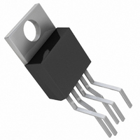
LT1764ET-2.5#06PBF Linear Technology, LT1764ET-2.5#06PBF Datasheet - Page 4

LT1764ET-2.5#06PBF
Manufacturer Part Number
LT1764ET-2.5#06PBF
Description
IC REG LDO 2.5V 3A TO220-5
Manufacturer
Linear Technology
Datasheet
1.LT1764EQ-2.5.pdf
(20 pages)
Specifications of LT1764ET-2.5#06PBF
Regulator Topology
Positive Fixed
Voltage - Output
2.5V
Voltage - Input
Up to 20V
Voltage - Dropout (typical)
0.34V @ 3A
Number Of Regulators
1
Current - Output
3A
Current - Limit (min)
3.1A
Operating Temperature
-40°C ~ 125°C
Mounting Type
Through Hole
Package / Case
TO-220-5 (Bent and Staggered Leads)
Lead Free Status / RoHS Status
Lead free / RoHS Compliant
Note 1: Stresses beyond those listed under Absolute Maximum Ratings
may cause permanent damage to the device. Exposure to any Absolute
Maximum Rating condition for extended periods may affect device
reliability and lifetime.
Note 2: The LT1764 regulators are tested and specified under pulse load
conditions such that T
Performance at – 40°C and 125°C is assured by design, characterization
and correlation with statistical process controls.
Note 3: The LT1764 (adjustable version) is tested and specified for these
conditions with the ADJ pin connected to the OUT pin.
Note 4. Operating conditions are limited by maximum junction
temperature. The regulated output voltage specification will not apply for
all possible combinations of input voltage and output current. When
operating at maximum input voltage, the output current range must be
limited. When operating at maximum output current, the input voltage
range must be limited.
Note 5: To satisfy requirements for minimum input voltage, the LT1764
(adjustable version) is tested and specified for these conditions with an
external resistor divider (two 4.12k resistors) for an output voltage of 2.42V.
The external resistor divider will add a 300µA DC load on the output.
LT1764 Series
ELECTRICAL CHARACTERISTICS
The
PARAMETER
GND Pin Current
V
(Notes 5, 7)
Output Voltage Noise
ADJ Pin Bias Current
Shutdown Threshold
SHDN Pin Current
(Note 9)
Quiescent Current in Shutdown
Ripple Rejection
Current Limit
Input Reverse Leakage Current
Reverse Output Current (Note 10) LT1764-1.5 V
4
IN
= V
●
OUT(NOMINAL)
denotes specifications which apply over the full operating temperature range, otherwise specifications are T
+ 1V
J
≈ T
A
. The LT1764 is 100% tested at T
CONDITIONS
I
I
I
I
I
I
I
C
(Notes 3, 8)
V
V
V
V
V
V
f
V
LT1764-1.8, LT1764-2.5, LT1764-3.3
V
V
LT1764, LT1764-1.5
V
V
V
LT1764-1.8 V
LT1764-2.5 V
LT1764-3.3 V
LT1764 (Note 3) V
LOAD
LOAD
LOAD
LOAD
LOAD
LOAD
LOAD
RIPPLE
OUT
OUT
OUT
SHDN
SHDN
IN
IN
IN
IN
IN
IN
IN
IN
= 6V, V
– V
= 7V, V
= V
= V
= 2.7V, ∆V
= 2.7V, ∆V
= – 20V, V
= 10µF, I
= Off to On
= On to Off
= 0mA
= 1mA
= 100mA
= 500mA
= 1.5A
= 2.7A, 110°C < T
= 3A, – 40°C ≤ T
= 0V
= 20V
OUT
OUT(NOMINAL)
OUT(NOMINAL)
= 120Hz, I
SHDN
OUT
= 1.5V (Avg), V
OUT
LOAD
OUT
OUT
OUT
OUT
OUT
OUT
= 0V
= 0V
LOAD
= 0V
= – 0.1V, – 40°C ≤ T
= – 0.1V, 110°C < T
= 1.5V, V
= 1.8V, V
= 2.5V, V
= 3.3V, V
OUT
= 3A, BW = 10Hz to 100kHz
+ 1V, ∆V
+ 1V, ∆V
J
= 1.5A
= 1.21V, V
J
≤ 110°C
≤ 125°C
A
RIPPLE
= 25°C.
IN
IN
IN
IN
OUT
OUT
< 1.5V
< 1.8V
< 2.5V
< 3.3V
= 0.5V
= – 0.1V, – 40°C ≤ T
= – 0.1V, 110°C < T
IN
< 1.21V
J
J
≤ 125°C
P-P
≤ 110°C
,
Note 6: Dropout voltage is the minimum input to output voltage differential
needed to maintain regulation at a specified output current. In dropout, the
output voltage will be equal to: V
Note 7: GND pin current is tested with V
V
current will decrease at higher input voltages.
Note 8: ADJ pin bias current flows into the ADJ pin.
Note 9: SHDN pin current flows into the SHDN pin.
Note 10: Reverse output current is tested with the IN pin grounded and the
OUT pin forced to the rated output voltage. This current flows into the OUT
pin and out the GND pin.
Note 11. For the LT1764, LT1764-1.5 and LT1764-1.8 dropout voltage will
be limited by the minimum input voltage specification under some output
voltage/load conditions.
Note 12. All combinations of absolute maximum input voltage and
absolute maximum output voltage cannot be achieved. The absolute
maximum differential from input to output is ±20V. For example, with
V
IN
IN
= 2.7V (whichever is greater) and a current source load. The GND pin
= 20V, V
J
J
≤ 125°C
≤ 110°C
OUT
cannot be pulled below ground.
●
●
●
●
●
●
●
●
IN
– V
0.25
MIN
3.1
2.8
3.1
2.8
55
DROPOUT
IN
= V
OUT(NOMINAL)
.
0.75
0.01
0.01
TYP
120
120
600
600
600
600
300
1.1
3.5
0.9
11
40
40
63
1
3
7
4
A
= 25°C. (Note 2)
1200
1200
1200
1200
MAX
+ 1V or
200
200
600
1.5
1.6
18
75
10
30
5
2
1
1
1
µV
UNITS
1764fb
RMS
mA
mA
mA
mA
mA
mA
mA
mA
µA
µA
µA
µA
dB
µA
µA
µA
µA
µA
V
V
A
A
A
A
A


