LP38692MPX-ADJ/NOPB National Semiconductor, LP38692MPX-ADJ/NOPB Datasheet - Page 12
LP38692MPX-ADJ/NOPB
Manufacturer Part Number
LP38692MPX-ADJ/NOPB
Description
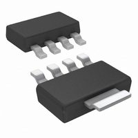
IC REG LDO 1A ADJ SOT223-5
Manufacturer
National Semiconductor
Series
PowerWise®r
Datasheet
1.LP38690SD-ADJNOPB.pdf
(16 pages)
Specifications of LP38692MPX-ADJ/NOPB
Regulator Topology
Positive Adjustable
Voltage - Output
1.25 ~ 9 V
Voltage - Input
2.7 ~ 10 V
Voltage - Dropout (typical)
0.45V @ 1A
Number Of Regulators
1
Current - Output
1A
Operating Temperature
-40°C ~ 125°C
Mounting Type
Surface Mount
Package / Case
SOT-223 (4 leads + Tab)
For Use With
LP38692EVAL - BOARD EVALUATION LP38692
Lead Free Status / RoHS Status
Lead free / RoHS Compliant
Current - Limit (min)
-
Other names
LP38692MPX-ADJ
Available stocks
Company
Part Number
Manufacturer
Quantity
Price


www.national.com
Application Hints
EXTERNAL CAPACITORS
Like any low-dropout regulator, external capacitors are re-
quired to assure stability. These capacitors must be correctly
selected for proper performance.
INPUT CAPACITOR: An input capacitor of at least 1µF is re-
quired (ceramic recommended). The capacitor must be lo-
cated not more than one centimeter from the input pin and
returned to a clean analog ground.
OUTPUT CAPACITOR: An output capacitor is required for
loop stability. It must be located less than 1 centimeter from
the device and connected directly to the output and ground
pins using traces which have no other currents flowing
through them.
The minimum amount of output capacitance that can be used
for stable operation is 1µF. Ceramic capacitors are recom-
mended (the LP38690/2-ADJ was designed for use with ultra
low ESR capacitors). The LP38690/2-ADJ is stable with any
output capacitor ESR between zero and 100 Ohms.
SETTING THE OUTPUT VOLTAGE: The output voltage is
set using the external resistors R1 and R2 (see Typical Ap-
plication Circuit). The output voltage will be given by the
equation:
Because the part has a minimum load current requirement of
100 µA, it is recommended that R2 always be 12k Ohms or
less to provide adequate loading. Even if a minimum load is
always provided by other means, it is not recommended that
very high value resistors be used for R1 and R2 because it
can make the ADJ node susceptible to noise pickup. A max-
imum value of 100k is recommended for R2 to prevent this
from occurring.
ENABLE PIN (LP38692-ADJ only):The LP38692–ADJ has
an Enable pin (EN) which allows an external control signal to
turn the regulator output On and Off. The Enable On/Off
threshold has no hysteresis. The voltage signal must rise and
fall cleanly, and promptly, through the ON and OFF voltage
thresholds. The Enable pin has no internal pull-up or pull-
down to establish a default condition and, as a result, this pin
must be terminated either actively or passively. If the Enable
pin is driven from a source that actively pulls high and low, the
drive voltage should not be allowed to go below ground po-
tential or higher than V
the Enable function, the pin should be connected directly to
the V
FOLDBACK CURRENT LIMITING: Foldback current limiting
is built into the LP38690/2-ADJ which reduces the amount of
output current the part can deliver as the output voltage is
reduced. The amount of load current is dependent on the dif-
ferential voltage between V
differential voltage exceeds 5V, the load current will limit at
about 450 mA. When the V
low 4V, load current is limited to about 1500 mA.
SELECTING A CAPACITOR
It is important to note that capacitance tolerance and variation
with temperature must be taken into consideration when se-
lecting a capacitor so that the minimum required amount of
capacitance is provided over the full operating temperature
range.
IN
pin.
V
OUT
= V
IN
ADJ
. If the application does not require
IN
x (1 + ( R1 / R2 ) )
IN
-V
and V
OUT
differential is reduced be-
OUT
. Typically, when this
12
Capacitor Characteristics
CERAMIC
For values of capacitance in the 10 to 100 µF range, ceramics
are usually larger and more costly than tantalums but give
superior AC performance for bypassing high frequency noise
because of very low ESR (typically less than 10 mΩ). How-
ever, some dielectric types do not have good capacitance
characteristics as a function of voltage and temperature.
Z5U and Y5V dielectric ceramics have capacitance that drops
severely with applied voltage. A typical Z5U or Y5V capacitor
can lose 60% of its rated capacitance with half of the rated
voltage applied to it. The Z5U and Y5V also exhibit a severe
temperature effect, losing more than 50% of nominal capac-
itance at high and low limits of the temperature range.
X7R and X5R dielectric ceramic capacitors are strongly rec-
ommended if ceramics are used, as they typically maintain a
capacitance range within ±20% of nominal over full operating
ratings of temperature and voltage. Of course, they are typi-
cally larger and more costly than Z5U/Y5U types for a given
voltage and capacitance.
TANTALUM
Solid Tantalum capacitors have good temperature stability: a
high quality Tantalum will typically show a capacitance value
that varies less than 10-15% across the full temperature
range of -40°C to 125°C. ESR will vary only about 2X going
from the high to low temperature limits.
The increasing ESR at lower temperatures can cause oscil-
lations when marginal quality capacitors are used (if the ESR
of the capacitor is near the upper limit of the stability range at
room temperature).
REVERSE VOLTAGE
A reverse voltage condition will exist when the voltage at the
output pin is higher than the voltage at the input pin. Typically
this will happen when V
tinues to hold a sufficient charge such that the input to output
voltage becomes reversed. A less common condition is when
an alternate voltage source is connected to the output.
There are two possible paths for current to flow from the out-
put pin back to the input during a reverse voltage condition.
1) While V
and the Enable pin (LP38692-ADJ only) is above the
V
the output voltage. If the input voltage is less than the pro-
grammed output voltage, the control circuit will drive the gate
of the pass element to the full ON condition. In this condition,
reverse current will flow from the output pin to the input pin,
limited only by the R
to input voltage differential. Discharging an output capacitor
up to 1000 μF in this manner will not damage the device as
the current will rapidly decay. However, continuous reverse
current should be avoided. When the Enable pin is low this
condition will be prevented.
2) The internal PFET pass element has an inherent parasitic
diode. During normal operation, the input voltage is higher
than the output voltage and the parasitic diode is reverse bi-
ased. However, when V
circuity is alive, or the Enable pin is low (LP38692-ADJ only),
and the output voltage is more than 500 mV (typical) above
the input voltage the parasitic diode becomes forward biased
and current flows from the output pin to the input pin through
the diode. The current in the parasitic diode should be limited
to less than 1A continuous and 5A peak.
EN(ON)
threshold, the control circuitry will attempt to regulate
IN
is high enough to keep the control circuity alive,
DS(ON)
IN
IN
is abruptly taken low and C
is below the value where the control
of the pass element and the output
OUT
con-
Related parts for LP38692MPX-ADJ/NOPB
Image
Part Number
Description
Manufacturer
Datasheet
Request
R

Part Number:
Description:
IC REG LDO 1A 1.8V SOT223-5
Manufacturer:
National Semiconductor
Part Number:
Description:
IC REG LDO 1A 2.5V SOT223-5
Manufacturer:
National Semiconductor
Part Number:
Description:
IC REG LDO 1A 3.3V SOT223-5
Manufacturer:
National Semiconductor
Part Number:
Description:
IC REG LDO 1A 5.0V SOT223-5
Manufacturer:
National Semiconductor

Part Number:
Description:
IC,VOLT REGULATOR,FIXED,+3.3V,CMOS,SOT-223-4,4PIN,PLASTIC
Manufacturer:
National Semiconductor
Part Number:
Description:
IC,VOLT REGULATOR,FIXED,+5V,CMOS,SOT-223-4,4PIN,PLASTIC
Manufacturer:
National Semiconductor
Part Number:
Description:
IC,VOLT REGULATOR,ADJUSTABLE,+1.25 TO +9V,CMOS,SOT-223-5,5PIN,PLASTIC
Manufacturer:
National Semiconductor
Part Number:
Description:
National Semiconductor [8-Bit D/A Converter]
Manufacturer:
National Semiconductor
Datasheet:
Part Number:
Description:
National Semiconductor [Media Coprocessor]
Manufacturer:
National Semiconductor
Datasheet:
Part Number:
Description:
Digitally Controlled Tone and Volume Circuit with Stereo Audio Power Amplifier, Microphone Preamp Stage and National 3D Sound
Manufacturer:
National Semiconductor
Datasheet:
Part Number:
Description:
Digitally Controlled Tone and Volume Circuit with Stereo Audio Power Amplifier, Microphone Preamp Stage and National 3D Sound
Manufacturer:
National Semiconductor
Datasheet:
Part Number:
Description:
AC97 Rev 2 Codec with Sample Rate Conversion and National 3D Sound
Manufacturer:
National Semiconductor
Part Number:
Description:
Manufacturer:
National Semiconductor
Datasheet:
Part Number:
Description:
Manufacturer:
National Semiconductor
Datasheet: