LMS8117ADT-3.3/NOPB National Semiconductor, LMS8117ADT-3.3/NOPB Datasheet - Page 4
LMS8117ADT-3.3/NOPB
Manufacturer Part Number
LMS8117ADT-3.3/NOPB
Description
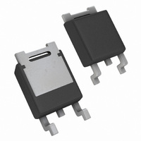
IC REGULATOR 1A LDO TO-252
Manufacturer
National Semiconductor
Type
Linearr
Datasheet
1.LMS8117AMPX-1.8NOPB.pdf
(16 pages)
Specifications of LMS8117ADT-3.3/NOPB
Regulator Topology
Positive Fixed
Voltage - Output
3.3V
Voltage - Input
Up to 15V
Voltage - Dropout (typical)
1.2V @ 1A
Number Of Regulators
1
Current - Output
1A
Current - Limit (min)
1A
Operating Temperature
0°C ~ 125°C
Mounting Type
Surface Mount
Package / Case
TO-252-2, DPak (2 Leads + Tab), TO-252AA, SC-63
Package
3TO-252
Function
LDO
Number Of Outputs
1
Input Voltage Range
15 to 2.5 V
Output Voltage
3.3 V
Maximum Output Current
1 A
Output Type
Fixed
Accuracy
±1 %
Typical Dropout Voltage @ Current
1.1@100mA|1.15@500mA|1.2@1A V
Polarity
Positive
Lead Free Status / RoHS Status
Lead free / RoHS Compliant
Other names
*LMS8117ADT-3.3
*LMS8117ADT-3.3/NOPB
LMS8117ADT-3.3
*LMS8117ADT-3.3/NOPB
LMS8117ADT-3.3
Available stocks
Company
Part Number
Manufacturer
Quantity
Price
Company:

Part Number:
LMS8117ADT-3.3/NOPB
Manufacturer:
TI
Quantity:
20 000


www.national.com
Electrical Characteristics
Symbol
Typicals and limits appearing in normal type apply for T
tion temperature range for operation, 0˚C to 125˚C.
Note 1: Absolute Maximum Ratings indicate limits beyond which damage to the device may occur. Operating Ratings indicate conditions for which the device is
intended to be functional, but specific performance is not guaranteed. For guaranteed specifications and the test conditions, see the Electrical Characteristics.
Note 2: The maximum power dissipation is a function of T
P
Note 3: For testing purposes, ESD was applied using human body model, 1.5kΩ in series with 100pF.
Note 4: Typical Values represent the most likely parametric norm.
Note 5: All limits are guaranteed by testing or statistical analysis.
Note 6: Load and line regulation are measured at constant junction room temperature.
Note 7: The dropout voltage is the input/output differential at which the circuit ceases to regulate against further reduction in input voltage. It is measured when the
output voltage has dropped 100mV from the nominal value obtained at V
Note 8: The minimum output current required to maintain regulation.
Note 9: Minimum pad size of 0.038in
D
= (T
J(MAX)
–T
Temperature Stability
Long Term Stability
RMS Output Noise
Thermal Resistance
Junction-to-Case
Thermal Resistance
Junction-to-Ambient
(No heat sink;
No air flow)
A
)/θ
JA
Parameter
. All numbers apply for packages soldered directly into a PC board.
2
T
(% of V
3-Lead SOT-223
3-Lead TO-252
3-Lead SOT-223
3-Lead TO-252 (Note 9)
A
= 125˚C, 1000Hrs
(Continued)
OUT
), 10Hz ≤ f ≤ 10kHz
J(MAX)
Conditions
, θ
J
JA
= 25˚C. Limits appearing in Boldface type apply over the entire junc-
IN
, and T
= V
OUT
4
A
. The maximum allowable power dissipation at any ambient temperature is
+1.5V.
(Note 5)
Min
(Note 4)
0.003
15.0
Typ
136
0.5
0.3
10
92
(Note 5)
Max
Units
˚C/W
˚C/W
˚C/W
˚C/W
%
%
%
Related parts for LMS8117ADT-3.3/NOPB
Image
Part Number
Description
Manufacturer
Datasheet
Request
R

Part Number:
Description:
IC,VOLT REGULATOR,FIXED,+3.3V,BIPOLAR,SIP,3PIN,PLASTIC
Manufacturer:
National Semiconductor

Part Number:
Description:
Linear Voltage Regulator IC
Manufacturer:
National Semiconductor
Datasheet:

Part Number:
Description:
1A Low-Dropout Linear Regulator
Manufacturer:
NSC [National Semiconductor]
Datasheet:

Part Number:
Description:
IC REGULATOR 1A LDO TO-252
Manufacturer:
National Semiconductor
Datasheet:
Part Number:
Description:
IC REG LINEAR LDO 1A 1.8V TO-252
Manufacturer:
National Semiconductor
Datasheet:
Part Number:
Description:
National Semiconductor [8-Bit D/A Converter]
Manufacturer:
National Semiconductor
Datasheet:
Part Number:
Description:
National Semiconductor [Media Coprocessor]
Manufacturer:
National Semiconductor
Datasheet:
Part Number:
Description:
Digitally Controlled Tone and Volume Circuit with Stereo Audio Power Amplifier, Microphone Preamp Stage and National 3D Sound
Manufacturer:
National Semiconductor
Datasheet:
Part Number:
Description:
Digitally Controlled Tone and Volume Circuit with Stereo Audio Power Amplifier, Microphone Preamp Stage and National 3D Sound
Manufacturer:
National Semiconductor
Datasheet:
Part Number:
Description:
AC97 Rev 2 Codec with Sample Rate Conversion and National 3D Sound
Manufacturer:
National Semiconductor
Part Number:
Description:
Manufacturer:
National Semiconductor
Datasheet:
Part Number:
Description:
Manufacturer:
National Semiconductor
Datasheet:
Part Number:
Description:
General Purpose, Low Voltage, Low Power, Rail-to-Rail Output Operational Amplifiers
Manufacturer:
National Semiconductor
Datasheet:
Part Number:
Description:
8-bit 20 MSPS flash A/D converter.
Manufacturer:
National Semiconductor
Datasheet: