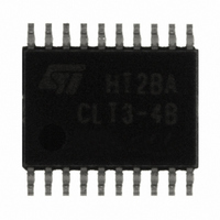
CLT3-4BT6-TR STMicroelectronics, CLT3-4BT6-TR Datasheet

CLT3-4BT6-TR
Specifications of CLT3-4BT6-TR
Available stocks
Related parts for CLT3-4BT6-TR
CLT3-4BT6-TR Summary of contents
Page 1
... Communication field bus nodes ■ Peripheral input / output modules ■ Machine tool interface Description The CLT3 quadruple input digital termination device designed for automation applications. It provides the front-end circuitry of a digital input module (I/O) in industrial automation, and drives an isolating opto-coupler. Figure 1. ...
Page 2
... OPTO COUPLER DRIVER OUT 1.5mA COM 12 1.5mA I 2 OUT 2 OPTO COUPLER DRIVER COM OPTO COUPLER DRIVER OUT 1.5mA COM 34 1.5mA I 4 OUT 4 OPTO COUPLER DRIVER Value = 0 kΩ 4.7 kΩ kΩ 1.2 kΩ 1.2 kΩ 150 Section 2.2. CLT3-4B Unit ° C ° C ...
Page 3
... CLT3-4B Table 2. Thermal resistance Symbol TSSOP20 thermal resistance junction to ambient R th(j-a) Board copper surface = 2 cm Table 3. Electrical characteristics (T referred unless otherwise specified) Symbol Pin I IN LIM V IN LOW OUT OFF V OUT OFF I OUT According to Figure 9: Robust application diagram on page 1.8 kΩ resistor, and an opto-coupler ( ...
Page 4
... The CLT3 quad channel device compatible the type 1 and 3 characteristics of the IEC 61131-2 standard. Each input voltage clamping block protects the module input against electromagnetic interferences such as those described in the IEC 61131-2 standard and IEC 61000-4-2 (ESD), 4-4 (transient burst), 4-5 (voltage surge) standards ...
Page 5
... R This document describes operation and characteristics for type 3 operation with and R ON MIN In type 1 operation the on state threshold set 2.2 kΩ. I 1.2 Input characteristics of CLT3-4 Figure 4. Typical input characteristics of each CLT3-4 channel V ( higher than the module input voltage Vi higher IN = 1.2 kΩ ...
Page 6
... Typical current limiter variation versus junction temperature 0.9 V < V < OUT I Iim / I Iim (25° C) 102% 100% 98% 96% 94% 92% 90% 88% 86 (°C) 84% - 1.3 CLT3-4 Input / output transfer characteristics (with respect to common pin COM) Figure 7. Current tranfer characteristic I (mA) OUT 4 3.5 3 Forbidden 2.5 2 1.5 1 0.04 0 0.5 1 1.5 ...
Page 7
... Figure 10) through its input protection diode while its opto-coupler remains OFF. Such a case is not critical for the CLT3-4 itself represents less than 15 mW per disturbed input. But the input resistors should be designed with care regardless of their thermal characteristics (refer to Application note AN2527). ...
Page 8
... Application information The CLT3-4 and the 24 V bus power supply have the same ground COM = GND. The reverse polarity of the power supply will shutdown the device. And the power supply resistor R will limit the default current protecting the power supply pin V C than 0 ...
Page 9
... Application information is biased and the REG N REG OUT OUT 1 1 OPTO OPTO N N OPTO OPTO 4 4 OUT OUT REG4 REG4 CLT3 - 4 CLT3 - 4 COM COM COM OUT OUT OUT COM COM COM OUT OUT OUT COM COM COM COM COM COM OUT ...
Page 10
... V C Figure 12). voltage surge test circuit C Ω PPI PPI Ω ± with 42 PPI PPI V V PPI PPI GND GND PE/FE PE/FE can be adjusted because of I Table 6. (kΩ) V surge (kV 2 Figure 12). withstands IEC 61000-4-5 with CLT3 -4 COM COM P P CLT3-4B ...
Page 11
... CLT3-4B 3 Package information ● Epoxy meets UL94,V0 In order to meet environmental requirements, ST offers these devices in ECOPACK® packages. These packages have a lead-free second level interconnect. The category of second level interconnect is marked on the package and on the inner box label, in compliance with JEDEC Standard JESD97. The maximum ratings related to soldering conditions are also marked on the inner box label ...
Page 12
... Ordering information 4 Ordering information Table 8. Ordering information Order code CLT3-4BT6 CLT3-4BT6-TR 5 Revision history Table 9. Document revision history Date August-2002 27-Nov-2007 12/13 Marking Package CLT3-4B TSSOP20 CLT3-4B TSSOP20 Revision 4A Previous release. Reformatted and restructured to current standard. Updated Figure 2, Figure 9, Figure 5 Added paragraphs to information ...
Page 13
... CLT3-4B Information in this document is provided solely in connection with ST products. STMicroelectronics NV and its subsidiaries (“ST”) reserve the right to make changes, corrections, modifications or improvements, to this document, and the products and services described herein at any time, without notice. All ST products are sold pursuant to ST’s terms and conditions of sale. ...


