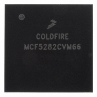
MCF5282CVM66 Freescale Semiconductor, MCF5282CVM66 Datasheet - Page 532

MCF5282CVM66
Manufacturer Part Number
MCF5282CVM66
Description
IC MPU 512K 66MHZ 256-MAPBGA
Manufacturer
Freescale Semiconductor
Series
MCF528xr
Datasheet
1.MCF5216CVM66J.pdf
(766 pages)
Specifications of MCF5282CVM66
Core Processor
Coldfire V2
Core Size
32-Bit
Speed
66MHz
Connectivity
CAN, EBI/EMI, Ethernet, I²C, SPI, UART/USART
Peripherals
DMA, LVD, POR, PWM, WDT
Number Of I /o
150
Program Memory Size
512KB (512K x 8)
Program Memory Type
FLASH
Ram Size
64K x 8
Voltage - Supply (vcc/vdd)
2.7 V ~ 3.6 V
Data Converters
A/D 8x10b
Oscillator Type
External
Operating Temperature
-40°C ~ 85°C
Package / Case
256-MAPBGA
Controller Family/series
ColdFire
No. Of I/o's
150
Ram Memory Size
64KB
Cpu Speed
66.67MHz
Embedded Interface Type
CAN, I2C, SPI, UART
No. Of Pwm Channels
8
Rohs Compliant
Yes
Lead Free Status / RoHS Status
Lead free / RoHS Compliant
Eeprom Size
-
Available stocks
Company
Part Number
Manufacturer
Quantity
Price
Company:
Part Number:
MCF5282CVM66
Manufacturer:
FREESCAL
Quantity:
152
Company:
Part Number:
MCF5282CVM66
Manufacturer:
Freescale Semiconductor
Quantity:
10 000
Part Number:
MCF5282CVM66
Manufacturer:
NXP/恩智浦
Quantity:
20 000
Company:
Part Number:
MCF5282CVM66J
Manufacturer:
Freescale Semiconductor
Quantity:
10 000
- Current page: 532 of 766
- Download datasheet (9Mb)
Chip Configuration Module (CCM)
4
27.5.3
The following subsection describes the CCM registers.
27.5.3.1 Chip Configuration Register (CCR)
27-4
Accessing an unimplemented address has no effect and causes a cycle termination transfer error.
14–11
10–8
Bits
Address
15
7
6
5
Reset
Field LOAD
R/W
Register Descriptions
PSTEN
MODE
Name
Note: The reset value of the LOAD and MODE fields is determined during reset configuration. The SZEN is
set for master mode and cleared for all other configurations. The BME bit is set to enable the bus monitor and
all other bits in the register are cleared at reset.
LOAD
SZEN
—
—
15
To safeguard against unintentionally activating test logic, write 0x0000 to
the above reserved location during initialization (immediately after reset) to
lock out test features. Setting any bits in the CCR may lead to unpredictable
results.
14
Pad driver load. The LOAD bit selects full or partial drive strength for selected pad output drivers.
0 Default drive strength.
1 Full drive strength.
Table 27-2
Reserved, should be cleared.
Chip configuration mode. This read-only field reflects the chip configuration mode.
000-101 Reserved.
110 Single-chip mode.
111 Master mode.
Reserved, should be cleared.
SIZ[1:0] enable. This read/write bit enables the SIZ[1:0] function of the external pins.
0 SIZ[1:0] function disabled.
1 SIZ[1:0] function enabled.
PST[3:0]/DDATA[3:0] enable. This read/write bit enables the Processor Status (PST) and Debug
0 PST/DDATA function disabled.
1 PST/DDATA function enabled.
For maximum capacitive load, set the LOAD bit to select full drive strength. For reduced power
consumption and reduced electromagnetic interference (EMI), clear the LOAD bit to select partial
drive strength.
Data (DDATA)n functions of the external pins.
R/W
MCF5282 and MCF5216 ColdFire Microcontroller User’s Manual, Rev. 3
—
Figure 27-2. Chip Configuration Register (CCR)
shows the read/write accessibility of this write-once bit.
Table 27-4. CCR Field Descriptions
11
10
Read Only
MODE
IPSBAR + 0x11_0004
NOTE
See Note
8
Description
—
7
SZEN PSTEN
6
5
—
4
R/W
BME
3
Freescale Semiconductor
2
BMT
0
Related parts for MCF5282CVM66
Image
Part Number
Description
Manufacturer
Datasheet
Request
R
Part Number:
Description:
Mcf5282 And Mcf5216 Coldfire Microcontroller User�s Manual
Manufacturer:
Freescale Semiconductor, Inc
Datasheet:
Part Number:
Description:
Manufacturer:
Freescale Semiconductor, Inc
Datasheet:
Part Number:
Description:
Manufacturer:
Freescale Semiconductor, Inc
Datasheet:
Part Number:
Description:
Manufacturer:
Freescale Semiconductor, Inc
Datasheet:
Part Number:
Description:
Manufacturer:
Freescale Semiconductor, Inc
Datasheet:
Part Number:
Description:
Manufacturer:
Freescale Semiconductor, Inc
Datasheet:
Part Number:
Description:
Manufacturer:
Freescale Semiconductor, Inc
Datasheet:
Part Number:
Description:
Manufacturer:
Freescale Semiconductor, Inc
Datasheet:
Part Number:
Description:
Manufacturer:
Freescale Semiconductor, Inc
Datasheet:
Part Number:
Description:
Manufacturer:
Freescale Semiconductor, Inc
Datasheet:
Part Number:
Description:
Manufacturer:
Freescale Semiconductor, Inc
Datasheet:
Part Number:
Description:
Manufacturer:
Freescale Semiconductor, Inc
Datasheet:
Part Number:
Description:
Manufacturer:
Freescale Semiconductor, Inc
Datasheet:
Part Number:
Description:
Manufacturer:
Freescale Semiconductor, Inc
Datasheet:
Part Number:
Description:
Manufacturer:
Freescale Semiconductor, Inc
Datasheet:


