MCIMX27ADSE Freescale Semiconductor, MCIMX27ADSE Datasheet
MCIMX27ADSE
Specifications of MCIMX27ADSE


Related parts for MCIMX27ADSE

MCIMX27ADSE Summary of contents
Page 1
... Freescale Semiconductor User’s Manual Development System © Freescale Semiconductor, Inc., 2006. All rights reserved. i.MX27 Application UMS-20956 Rev A, 08/2006 User’s Manual ...
Page 2
... Freescale Semiconductor product could create a situation where personal injury or death may occur. Should Buyer ...
Page 3
... Chapter 1 General Information 1.1 Description . . . . . . . . . . . . . . . . . . . . . . . . . . . . . . . . . . . . . . . . . . . . . . . . . . . . . . . . . . . . . . . . . 1-1 1.2 MCIMX27ADSE Features . . . . . . . . . . . . . . . . . . . . . . . . . . . . . . . . . . . . . . . . . . . . . . . . . . . . . 1-1 1.3 System and User Requirements . . . . . . . . . . . . . . . . . . . . . . . . . . . . . . . . . . . . . . . . . . . . . . . . . 1-2 1.4 MCIMX27ADSE Diagram . . . . . . . . . . . . . . . . . . . . . . . . . . . . . . . . . . . . . . . . . . . . . . . . . . . . . 1-3 1.5 ADS Specifications 1-6 Chapter 2 Configuration and Operation 2.1 Introduction 2-1 2.2 Configuring Board Components . . . . . . . . . . . . . . . . . . . . . . . . . . . . . . . . . . . . . . . . . . . . . . . . . 2-1 2.2.1 DIP Switch S7 - Li-Cell select switch . . . . . . . . . . . . . . . . . . . . . . . . . . . . . . . . . . . . . . . . . 2-1 2 ...
Page 4
... SD/MMC Connectors . . . . . . . . . . . . . . . . . . . . . . . . . . . . . . . . . . . . . . . . . . . . . . . . . . . . . . . . 3-16 3.14 Memory Stick Connector . . . . . . . . . . . . . . . . . . . . . . . . . . . . . . . . . . . . . . . . . . . . . . . . . . . . . 3-17 3.15 PCMCIA Connector . . . . . . . . . . . . . . . . . . . . . . . . . . . . . . . . . . . . . . . . . . . . . . . . . . . . . . . . . 3-17 3.16 ATA Connector 3-20 3.17 ETM Connector . . . . . . . . . . . . . . . . . . . . . . . . . . . . . . . . . . . . . . . . . . . . . . . . . . . . . . . . . . . . 3-22 3.18 CPLD Programming Connector . . . . . . . . . . . . . . . . . . . . . . . . . . . . . . . . . . . . . . . . . . . . . . . . 3-24 3.19 Audio Jacks 3-24 3.20 Extension and Image Sensor Connectors . . . . . . . . . . . . . . . . . . . . . . . . . . . . . . . . . . . . . . . . . 3-26 ii MCIMX27ADSE User’s Manual, Rev. A Freescale Semiconductor ...
Page 5
... The following table summarizes changes to this document since the previous release (Rev. A). Revision A Conventions Units and measures in this manual conform to the International System of Units (SI) as defined by National Institute of Standards and Technology Special Publication 811. Freescale Semiconductor Table 0-1. Revision History Description First release MCIMX27ADSE User’s Manual, Rev. A iii ...
Page 6
... Disposal Information This symbol means this product may be subject to special disposal requirment. For product disposal information, please refer to http://www.freescale.com/productdisposal. iv MCIMX27ADSE User’s Manual, Rev. A Freescale Semiconductor ...
Page 7
... Multi-chip package Mini-AB USB receptacle for mini-A plug and mini-B plug MMC Multi-media Card MS Memory Stick NAND Negative AND NVDD Noisy Supply OTG On the Go PC Personal Computer PCMCIA Personal Computer Memory Card International Association Freescale Semiconductor MCIMX27ADSE User’s Manual, Rev ...
Page 8
... System International (international system of units and measures) SPST SW Single Pole Single Throw Switch SSI Synchronous Serial Interface TFT Thin Film Transistor UART Universal Asynchronous Receiver/Transmitter USB Universal Serial Bus USB OTG Universal Serial Bus On-The-Go VDC Volts Direct Current vi MCIMX27ADSE User’s Manual, Rev. A Freescale Semiconductor ...
Page 9
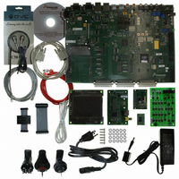
... The i.MX27 Application Development System (MCIMX27ADSE development tool which is designed to run software applications designed for i.MX27 microcontroller unit. The MCIMX27ADSE includes a main board, an LCD display panel, a keypad, a NAND flash card, an image sensor encoder card, etc. It supports application software, target-board debugging or optional extra memory ...
Page 10
... A Multi-ICE device (not included with your ADS) • VDC power supply @ 5A, with female (inside positive) power connector (included in your ADS) Never supply more than 5.5 volt power to your MCIMX27ADSE. Doing so can damage board components. 1-2 CAUTION MCIMX27ADSE User’s Manual, Rev. A ...
Page 11
... S16 J71 P13 U7 S2 P18 U59 P17 J16 Figure 1-1. MCIMX27ADSE Application Development System Important components on the top side of ADS are: • BZ1 — Buzzer • CN5 — Battery connector • D3 — 5 volt power LED (green) • D4 — MC13783 power LED (green) • ...
Page 12
... JP71, JP72 — 1.8V (NVDD2~4) Power enable for logic analyzer connector (P8, P9) • JP73 — Jumper for microphone input • P8, P9 — connections to Logic Analyzer • P14 — LCD panel connector • P15 — TV Encoder connector • P22 — Keypad module connector 1-4 MCIMX27ADSE User’s Manual, Rev. A Freescale Semiconductor ...
Page 13
... J16 — Memory Stick card connector • P13 — ATA Hard Disk Drive Connector • P17 — SD/MMC1 card connector • P18 — SD/MMC2 card connector • J92 — USB OTG (Full Speed) connector for MC13783 Freescale Semiconductor MCIMX27ADSE User’s Manual, Rev. A General Information 1-5 ...
Page 14
... Power requirements Dimensions 1-6 Table 1-1. Specifications Specifications CPU 400MHz, System 133MHz 10/100Base-T (RJ-45), RS-232 serial, USB HOST, USB OTG 0° to +50° C -40° to +85° 90% (noncondensing) — 4.75V 5.25 VDC @ 8.5 in (30.5 x 21.6 cm) MCIMX27ADSE User’s Manual, Rev. A Freescale Semiconductor ...
Page 15
... OFF OFF ON Table 2-2. Boot Mode Switch Settings Boot0 Boot1 S18-1 S18 OFF OFF OFF ON ON OFF ON ON OFF OFF OFF MCIMX27ADSE User’s Manual, Rev. A Configuration and Operation S7-3 S7-4 ON OFF OFF OFF OFF ON OFF OFF Boot2 Boot3 S18-3 S18 ...
Page 16
... Table 2-4. MC13783 USB Mode Switches S9-1 OFF ON OFF OFF NOTE Table 2-5. MC13783 CLIA Source Select S3-1 ON OFF OFF Table 2-6. MC13783 CLIB Source Select S3-2 ON OFF OFF MCIMX27ADSE User’s Manual, Rev. A Effect S9-2 S9-3 S9-4 OFF ON OFF OFF OFF ON ON OFF ON OFF OFF ON ...
Page 17
... Table 2-9. ADS Jumper Headers Pin Connection 1-2 Enable the EEPROM (U45) for the External Ethernet; default factory setting. 2-3 Disable the EEPROM (U45) for the External Ethernet. 1-2 Enable the SD/MMC2. MCIMX27ADSE User’s Manual, Rev. A Configuration and Operation Effect Effect Effect 2-3 ...
Page 18
... Handset earpiece speaker amplifier negative output. 1 Connect to the positive terminal of external Li-Cell. 2 Connect to the negative terminal of external Li-Cell. 1 External clock input for MC13783 audio bus 2 Ground 1 External microphone input for MC13783 MC2IN 2 Ground MCIMX27ADSE User’s Manual, Rev. A Effect Description Freescale Semiconductor ...
Page 19
... A/D LED drivers Backlight Convertor Touchscreen Interface Sharp LCD TV Encoder Connector CSI Connector Two Expansion Conn. 6x6 Keypad Buzzer One Wire EEPROM Figure 2-1. Functional Block Diagram of MCIMX27ADSE Freescale Semiconductor 1.5V Buck 2A 1.8V Buck 2B DVDD1.8V VRF1 CVDD_2.775V VRF2 CVDD_2.775V_1 2.775V ...
Page 20
... FCE CS1_B FCE2 EB0_B LB EB1_B HB WAIT_B RDY BCLK CLI OE_B OE LBA_B ADV RW_B WE FLASH_RST_B RST A[25:0] A[25:0] D[15:0] D[15:0] CS5_B PCE Figure 2-2. Burst Flash Interface MCIMX27ADSE User’s Manual, Rev. A Memory Size (Byte) 128M 32M 16M - - - U28 PSRAM Freescale Semiconductor ...
Page 21
... BA0 SDBA1 BA1 DQM0 LDM DQM1 UDM DSQ0 LDQS DSQ1 UDQS A[13:0] SDA[13:0] SD[15:0] D[15:0] DQM2 DQM3 DSQ2 DSQ3 SD[31:16] Figure 2-3. DDR SDRAM Interface MCIMX27ADSE User’s Manual, Rev. A Configuration and Operation U20 LDM U21 UDM LDQS UDQS D[15:0] 2-7 ...
Page 22
... USB host. The interface provides power on the USB bus. This power may 2 ISP1301BS (U37) VBUS ID ENA MIC2536 (U35) FLGA Figure 2-4. USB OTG (FS) Interface D- D+ ISP1504BS (U36) VBUS ID MIC2536 (U36) Figure 2-5. USB OTG (HS) Interface NOTE MCIMX27ADSE User’s Manual, Rev. A Mini AB (J10) Mini AB (J9) Freescale Semiconductor ...
Page 23
... Mux and enable controls of IrDA can be software controlled through the CPLD. Freescale Semiconductor D- D+ ISP1504BS (U30) VBUS ID MIC2536 (U33) Figure 2-6. USB Host (HS) Interface D- D+ ISP1105W (U34) VBUS ID ENA MIC2536 (U33) FLGA Figure 2-7. USB Host (HS) Interface MCIMX27ADSE User’s Manual, Rev. A Configuration and Operation USB A (J7) USB A (J8) 2-9 ...
Page 24
... Figure 2-8. UARTs and IrDA Interface CS8900A SA[12:1] (U44) SD[15:0] AEN IOR IOW MEMR MEMW SBHE CHIPSEL EEDATAIN INTRQ0 EEDATAOUT DMARQ0 EECS RESET HWSLEEP Figure 2-9. External Ethernet Interface MCIMX27ADSE User’s Manual, Rev. A UART A (J78) UART A (J79) IrDA (U7) RJ45 TX Connector RX (T1) EEPROM (U45) Freescale Semiconductor ...
Page 25
... U49, U50, U51) FEC signals MII R501 CS8900 DMA GPIO RQ i.MX27 (U1) RTCK/OWIRE DATA OWIRE JP62 RTCK RTCK_JTAG MCIMX27ADSE User’s Manual, Rev. A Configuration and Operation ATA module NetPHY RJ45 AM79C874 Connector (U48) (T3) CPLD (U92) 1-Wire EEPROM (U98) Multi-ICE Connector J89 ...
Page 26
... The ADS includes an audio indicator or buzzer, BZ1 jumper is installed in header JP63 pin 1-2, the PWMO pin of the i.MX27 controls this function. This buzzer operates from 1 KHz to 10 KHz. The maximum sound level is reached when the frequency is 3 KHz and the duty cycle is 50%. 2-12 MCIMX27ADSE User’s Manual, Rev. A Freescale Semiconductor ...
Page 27
... User status controlled by CPLD STAT 1 User status controlled by CPLD - Blinking indicates LAN Activity - Link good or host controlled output - Blinking indicates external bus activity LENLNK Blinking indicates LAN Activity LEDRX Blinking when data is received MCIMX27ADSE User’s Manual, Rev. A Configuration and Operation Function 2-13 ...
Page 28
... LCD module and/or the main board. 2-14 NAND Flash Card PN2 PN1 P9 PM2 PM2 PM1 i.MX27ADS J13 J14 Figure 2-12. Installing the NAND flash card CAUTION CAUTION MCIMX27ADSE User’s Manual, Rev. A JP63 J24 BZ1 S15 Freescale Semiconductor ...
Page 29
... Freescale Semiconductor JP73 CN5 J91 J11 JP65 P14 34 CONDUCTOR RIBBON CABLE P15 VR1 P22 Figure 2-13. Installing the LCD board MCIMX27ADSE User’s Manual, Rev. A Configuration and Operation LCD BOARD TFT LCD PANEL (240 x 320 dots) 2-15 ...
Page 30
... SW33 P14 P15 20 CONDUCTOR RIBBON CABLE P22 P1 Send Home App1 Vol Up Vol Down Extra 1 Power Record Figure 2-14. Installing the keypad MCIMX27ADSE User’s Manual, Rev. A KCOL2 KCOL1 KCOL0 UP KEY 2 END SW4 SW5 SW6 ACTION RIGHT BACK SW10 SW11 SW12 2 ABC ...
Page 31
... Connecting the card with power applied can damage the TV encoder card and the ADS board. Freescale Semiconductor 2 C interface. For details on image sensor CAUTION P8 P9 PM2 i.MX27ADS J13 CAUTION MCIMX27ADSE User’s Manual, Rev. A Configuration and Operation PM1 S15 J14 2-17 ...
Page 32
... Since the signals of the memory stick and SD/MMC2 are multiplexed in i.MX27, it cannot use both memory cards at the same time. 2-18 CN5 R425 J91 JP65 P14 P15 P22 J14 Figure 2-16. Installing the TV Encoder Card NOTE MCIMX27ADSE User’s Manual, Rev Freescale Semiconductor ...
Page 33
... The ADS has two specialized Samtec connectors (P8 and P9) designed to be compatible with Logic Analyzer cables from HP that use the mating connector. All CPU connections required for memory interfacing are brought to these connectors. Freescale Semiconductor CAUTION MCIMX27ADSE User’s Manual, Rev. A Configuration and Operation 2-19 ...
Page 34
... Configuration and Operation 2-20 MCIMX27ADSE User’s Manual, Rev. A Freescale Semiconductor ...
Page 35
... Logic Analyzer Connectors P8 and P9 are the logic analyzer connectors. All are 100-pin SAMTEC connectors. Figure 3-1 shows P8 pin assignments and Table 3-1 describes P8 signals. Figure 3-2 shows P9 pin assignments and Table 3-2 describes P9 signals. Freescale Semiconductor MCIMX27ADSE User’s Manual, Rev. A 3-1 ...
Page 36
... GND • • • • GND 85 86 GND • • • • GND 89 90 GND • • • • GND 93 94 GND • • GND 95 96 GND • • • • NVDD2~4 99 100 NC MCIMX27ADSE User’s Manual, Rev. A Freescale Semiconductor ...
Page 37
... RESET OUT - Active low reset signal from the MCU PM_RESETB_MCU POWER MANAGEMENT MCU POWER ON RESET PM_RESETB POWER MANAGEMENT MCU RESET BCLK CLOCK SIGNAL FOR BURST FLASH PC_POE PCMCIA CONTROL NVDD2~4 EMI INTERFACE POWER SUPPLY MCIMX27ADSE User’s Manual, Rev. A Support Information Description 3-3 ...
Page 38
... GND • • • • GND 88 86 GND • • • • GND 89 90 GND • • • • GND 93 94 GND • • GND 95 96 GND • • • • NVDD2~4 99 100 NC MCIMX27ADSE User’s Manual, Rev. A Freescale Semiconductor ...
Page 39
... NAND FLASH CONTROL NFCLE NAND FLASH CONTROL NFALE NAND FLASH CONTROL NFRE_B NAND FLASH CONTROL NFWP_B NAND FLASH CONTROL NFWE_B NAND FLASH CONTROL NFRB_B NAND FLASH CONTROL NVDD2~4 EMI INTERFACE POWER SUPPLY MCIMX27ADSE User’s Manual, Rev. A Support Information Description 3-5 ...
Page 40
... This male DB9 connector is configured for RS-232 DTE operation. Figure 3-4 shows pin assignments and Table 3-4 provides signal descriptions for the connector. Figure 3-4. Connector J79 (UART4) DTE Pin Assignments 3 J78 Description J79 MCIMX27ADSE User’s Manual, Rev. A Figure 3-1 Freescale Semiconductor ...
Page 41
... RING INDICATOR — RS-232 output signal, forced inactive negative 3.4 Multi-ICE Connector Connector J89 is the ADS Multi-ICE connector. Figure 3-6 shows pin assignments and Table 3-6 provides signal descriptions for the connector. Freescale Semiconductor Description J80 Description MCIMX27ADSE User’s Manual, Rev. A Support Information 3-7 ...
Page 42
... TCK 9 10 GND • • RTCK 11 12 GND • • TDO 13 14 GND • • PM_RESETB 15 16 GND • • GND • • GND Description 1 8 Pin(s) Signal Description 1 TPO+ DIFFERENTIAL OUTPUT PLUS MCIMX27ADSE User’s Manual, Rev. A Freescale Semiconductor ...
Page 43
... Figure 3-8. FEC Connector T3 Pin Numbers Signal Description TPO+ DIFFERENTIAL OUTPUT PLUS TPO- DIFFERENTIAL OUTPUT MINUS TPI+ DIFFERENTIAL INPUT PLUS - CENTER TAP OF DIFFERENTIAL OUTPUT - CENTER TAP OF DIFFERENTIAL INPUT TPI- DIFFERENTIAL INPUT MINUS NC NO CONNECTION GND GROUND MCIMX27ADSE User’s Manual, Rev. A Support Information 3-9 ...
Page 44
... Table 3-10. USB Host Connector J7 and J8 Signal Descriptions 3- Pin(s) Signal Description 1 VBUS VBUS 2 D- USB DATA MINUS 3 D+ USB DATA PLUS GND GROUND 1 4 Pin(s) Signal Description 1 VBUS VBUS 2 D- USB DATA MINUS 3 D+ USB DATA PLUS GND GROUND MCIMX27ADSE User’s Manual, Rev. A Freescale Semiconductor ...
Page 45
... Test point BUFFERED NAND FLASH CHIP ENABLE +3.15 VDC power BUFFERED NAND FLASH COMMAND LATCH ENABLE BUFFERED NAND FLASH ADDRESS LATCH ENABLE BUFFERED NAND FLASH WRITE ENABLE BUFFERED NAND FLASH WRITE PROTECT GROUND MCIMX27ADSE User’s Manual, Rev. A Support Information 3-11 ...
Page 46
... NAND FLASH DATA BUS NAND FLASH DATA BUS NAND FLASH DATA BUS NAND FLASH DATA BUS NAND FLASH DATA BUS NAND FLASH DATA BUS NAND FLASH DATA BUS NAND FLASH DATA BUS NAND FLASH DATA BUS GROUND MCIMX27ADSE User’s Manual, Rev. A Freescale Semiconductor ...
Page 47
... KEYPAD COLUMN 1 — Bidirectional signal used to scan a keypad KEYPAD ROW 1 — Bidirectional signal used to scan a keypad KEYPAD COLUMN 0 — Bidirectional signal used to scan a keypad KEYPAD ROW 0 — Bidirectional signal used to scan a keypad GROUND MCIMX27ADSE User’s Manual, Rev. A Support Information Description 3-13 ...
Page 48
... SPL_SPR 21 22 REV • • CLS • • LD1 25 26 LD0 • • LD7 27 28 LD6 • • LD13 29 30 LD12 • • TOP 31 32 BOTTOM • • LEFT 33 34 RIGHT Description MCIMX27ADSE User’s Manual, Rev. A Freescale Semiconductor ...
Page 49
... Description 3V15 +3.15 VDC power 5V +5 VDC power I2C_CLK I SQUARED C CLOCK — Serial clock, bidirectional NC NO CONNECTION I2C_DATA I SQUARED C DATA — Serial data, bidirectional GND GROUND CLK_26M 26M Clock signal from TV encoder card MCIMX27ADSE User’s Manual, Rev. A Support Information 3-15 ...
Page 50
... GROUND DATA LINE 0 DATA LINE 1 INTERRUPT (IRQ) DATA LINE 2 READWAIT (RW) CARD DETECT FROM CPLD GROUND NO CONNECTION WRITE PROTECT DETECT FROM CPLD MCIMX27ADSE User’s Manual, Rev Card 4-Bit Mode DATA LINE 3 DATA LINE 1 or IRQ DATA LINE 2or IRQ Freescale Semiconductor ...
Page 51
... CARD DETECT MSHC_DATA3 DATA BUS MSHC_SCLK CLOCK SIGNAL 3V15 +3.15V POWER GND GROUND SIGNAL Description SIGNAL GROUND DATA 3 DATA 4 DATA 5 MCIMX27ADSE User’s Manual, Rev. A Support Information SD Card 4-Bit Mode DATA LINE 3 DATA LINE 1 or IRQ DATA LINE 2or IRQ 3-17 ...
Page 52
... ADDRESS 3 ADDRESS 2 ADDRESS 1 ADDRESS 0 DATA 0 DATA 1 DATA 2 PCMCIA control signal SIGNAL GROUND SIGNAL GROUND PCMCIA Card Detect 1 DATA 11 DATA 12 DATA 13 DATA 14 DATA 15 PCMCIA CARD ENABLE2 PCMCIA Voltage Sense 1 signal INPUT/OUTPUT READ INPUT/OUTPUT WRITE ADDRESS 17 MCIMX27ADSE User’s Manual, Rev. A Freescale Semiconductor ...
Page 53
... ADDRESS 23 ADDRESS 24 ADDRESS 25 PCMCIA Voltage Sense 2signal PCMCIA RESET PCMCIA WAIT NO CONNECTION PCMCIA REGISTER ACCESS OUTPUT PCMCIA Battery Voltage Detect 2 PCMCIA Battery Voltage Detect 1 DATA 8 DATA 9 DATA 10 PCMCIA Card Detect 2 SIGNAL GROUND NO CONNECTION MCIMX27ADSE User’s Manual, Rev. A Support Information 3-19 ...
Page 54
... ATA RESET SIGNAL GROUND SIGNAL ATA DATA BUS ATA DATA BUS ATA DATA BUS ATA DATA BUS ATA DATA BUS ATA DATA BUS ATA DATA BUS ATA DATA BUS ATA DATA BUS ATA DATA BUS MCIMX27ADSE User’s Manual, Rev. A Description Freescale Semiconductor ...
Page 55
... ATA REGISTER ADDRESS SIGNAL ATA REGISTER ADDRESS SIGNAL ATA CHIP SELECT ATA CHIP SELECT ATA DRIVE 1 IS PRESENT GROUND SIGNAL +3.3VDC POWER SUPPLY FOR LOGIC CIRCUIT +3.3VDC POWER SUPPLY FOR MOTOR GROUND SIGNAL GROUND SIGNAL MCIMX27ADSE User’s Manual, Rev. A Support Information 3-21 ...
Page 56
... NO CONNECTION NO CONNECTION NO CONNECTION NO CONNECTION GROUND SIGNAL ETM TRACE CLOCK TRACE REQUEST ETM DEBUG ACKNOWLEDGE RESET SIGNAL ETM EXTERNAL TRIGGER INPUT JTAG DATA OUT LOGIC LEVEL REFERENCE VOLTAGE FROM TARGET SYSTEM JTAG RETURN CLOCK MCIMX27ADSE User’s Manual, Rev. A Description Freescale Semiconductor ...
Page 57
... TRACE DATA TRACE DATA TRACE DATA TRACE SYNCHRONIZATION TRACE DATA TRACE PIPLINE STATUS TRACE DATA TRACE PIPLINE STATUS TRACE DATA TRACE PIPLINE STATUS GROUND SIGNAL GROUND SIGNAL GROUND SIGNAL GROUND SIGNAL GROUND SIGNAL NO CONNECTION MCIMX27ADSE User’s Manual, Rev. A Support Information 3-23 ...
Page 58
... TMS 3 4 GND • • TDI 5 6 3V15 • • TDO 7 8 GND • • Description JTAG CLOCK GROUND JTAG MODE GROUND JTAG DATA IN +3.15V POWER JTAG DATA OUT GROUND NO CONNECTION NO CONNECTION MCIMX27ADSE User’s Manual, Rev. A Freescale Semiconductor ...
Page 59
... HEADSET ANALOG OUTPUT RIGHT HSDETL HEADSET DETECT MIC MICROPHONE INPUT FROM JUMPER (JP73 CONNECTION Freescale Semiconductor Termination 2 3 MC1LIN MC1RIN HSR HSL RXOUTR RXOUTL RXINR RXINL Signal Description Termination 2 3 MC2IN PM_HSR HSDETL Signal Description MCIMX27ADSE User’s Manual, Rev. A Support Information MIC NC 3-25 ...
Page 60
... NO CONNECTION NO CONNECTION NO CONNECTION NO CONNECTION NO CONNECTION CSI Power Supply GROUND CSPI3 Master Out Slave In — bidirectional signal CSPI3 Master In Slave Out — bidirectional signal CSPI3 Clock — bidirectional signal CSPI3 Slave Select — bidirectional signal MCIMX27ADSE User’s Manual, Rev Freescale Semiconductor ...
Page 61
... I SQUARED C DATA — Serial data, bidirectional NO CONNECTION CMOS SENSOR CONTORL 0 — Control output from CPLD CMOS SENSOR CONTORL 1 — Control output from CPLD CMOS SENSOR CONTORL 2 — Control output from CPLD NO CONNECTION NO CONNECTION NO CONNECTION CSI Power Supply MCIMX27ADSE User’s Manual, Rev. A Support Information 3-27 ...
Page 62
... KEYPAD COLUMN 1 — Bidirectional signal used to scan a keypad B12 KP_COL0 KEYPAD COLUMN 0 — Bidirectional signal used to scan a keypad B13 SSI4_RXD SYCHRONOUS SERIAL INTERFACE 4 RECEIVED DATA — Serial input signal B14 SSI4_FS SYCHRONOUS SERIAL INTERFACE 4 FRAME SYNC 3-28 Description MCIMX27ADSE User’s Manual, Rev. A Freescale Semiconductor ...
Page 63
... CSPI2 SERIAL CLOCK — CSPI signal (bidirectional) CSPI2 SLAVE SELECT 0 — CSPI signal (bidirectional) CSPI2 SLAVE SELECT 1 — CSPI signal (bidirectional) CSPI2 SLAVE SELECT 2 — CSPI signal (bidirectional CLOCK — Serial clock, bidirectional DATA — Serial data, bidirectional MCIMX27ADSE User’s Manual, Rev. A Support Information 3-29 ...
Page 64
... TEST POINT TEST POINT TEST POINT TEST POINT TEST POINT USB Full Speed Host Transceiver On from CPLD GROUND TIMER INPUT CAPTURE — Timer input TIMER OUTPUT COMPARE — Timer output TEST POINT TEST POINT MCIMX27ADSE User’s Manual, Rev. A Freescale Semiconductor ...
Page 65
... PULSE WIDTH MODULATOR OUTPUT RESET OUT — Active low reset signal from the processor TEST POINT USB OVER CURRENT input active low USB POWER USB BY PASS input active low from CPLD +3.15 VDC power MCIMX27ADSE User’s Manual, Rev. A Support Information 3-31 ...
Page 66
... Support Information 3-32 MCIMX27ADSE User’s Manual, Rev. A Freescale Semiconductor ...
Page 67
...
Page 68
... Freescale Semiconductor product could create a situation where personal injury or death may occur. Should Buyer ...